Image sensor and formation method thereof
A technology of image sensor and photosensitive area, which is applied in the direction of electric solid-state devices, semiconductor devices, electrical components, etc., can solve the serious problems of CMOS image sensor process difficulty, optical crosstalk, etc., and achieve the effect of improving sensitivity and reducing influence
- Summary
- Abstract
- Description
- Claims
- Application Information
AI Technical Summary
Problems solved by technology
Method used
Image
Examples
Embodiment Construction
[0026] There are many problems in the image sensor, for example, the dark current of the image sensor is relatively large.
[0027] Now in conjunction with a CMOS image sensor, analyze the reason why the dark current of the CMOS image sensor is relatively large:
[0028] figure 1 It is a schematic diagram of the structure of a CMOS image sensor.
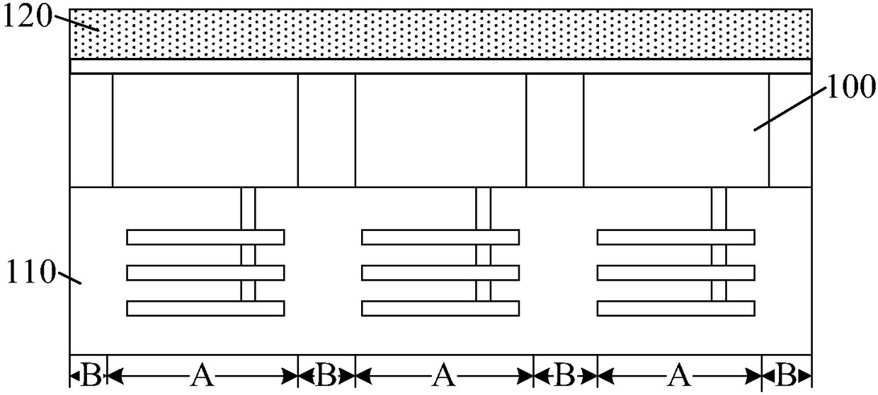
[0029] Please refer to figure 1 , the CMOS image sensor includes: a substrate 100, the substrate 100 includes an opposite first surface and a second surface, the substrate includes a plurality of discrete photosensitive regions A and adjacent photosensitive regions A Isolation region B; the second surface of the substrate 100 has a dielectric layer 110 .
[0030] Continuing with reference to 1, a metal layer 120 is formed on the first surface of the substrate 100 .
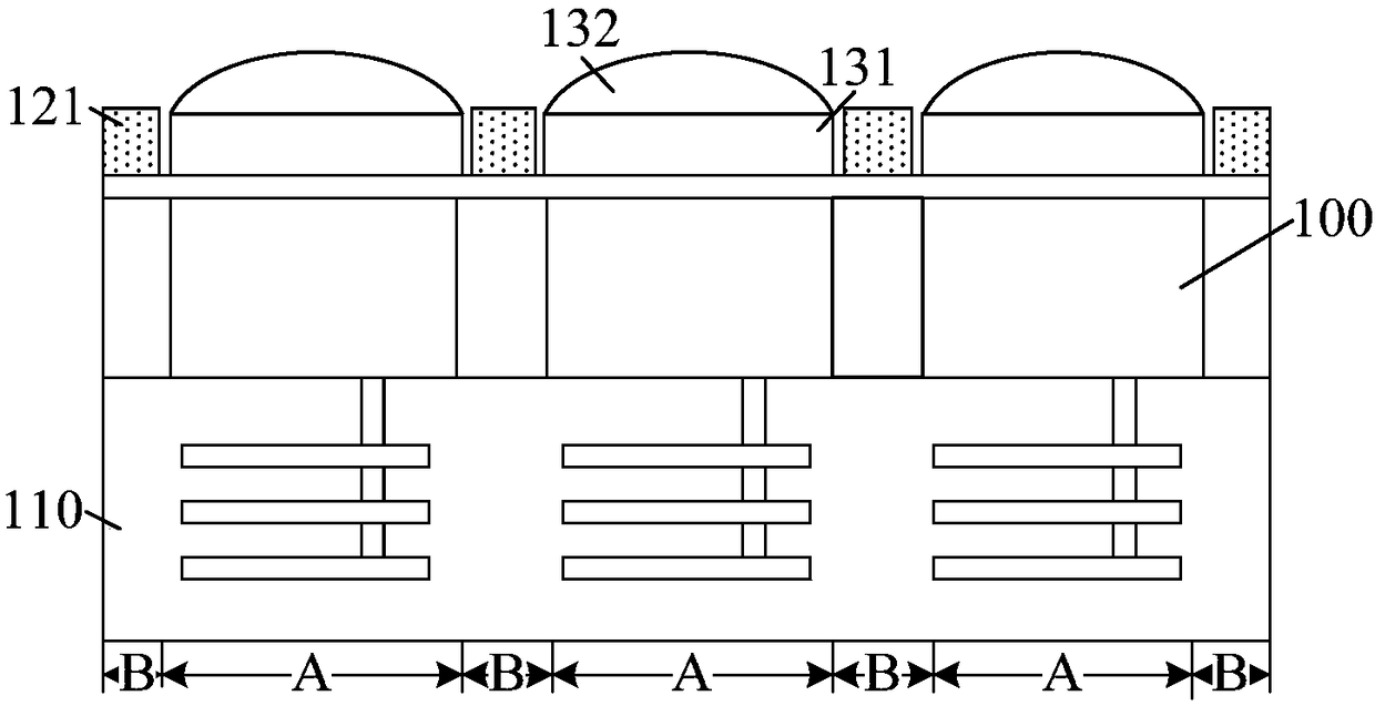
[0031] Please refer to figure 2 , the metal layer 120 is etched to remove the metal layer 120 in the isolation region B to form a metal grid 121; a filter 131 is f...
PUM
 Abstract
Description
Claims
Application Information


