Check patentability & draft patents in minutes with Patsnap Eureka AI!

flash memory

A technology of flash memory and flash memory unit, which is applied to semiconductor devices, electrical components, circuits, etc., and can solve the problems of increasing polysilicon floating gate mutual interference, information error, and reducing the spacing of polysilicon floating gates, etc.

Active Publication Date: 2021-06-15
SHANGHAI HUALI MICROELECTRONICS CORP
View PDF0 Cites 0 Cited by
  • Summary
  • Abstract
  • Description
  • Claims
  • Application Information

AI Technical Summary

Problems solved by technology

However, with the application of high-node technology, the situation that the width of the polysilicon floating gate is greater than the width of the active area will bring greater adverse effects, especially in the scaling down of the size, which usually affects the active area and field oxidation. The width of the layer is reduced proportionally, and the size of the pad oxide layer will not change, so the consumption of the field oxide layer caused by the etching of the pad oxide layer will change the size of the active region and occupy the width of the active region The ratio will gradually increase
The situation that the width of the polysilicon floating gate is greater than the width of the active region will make the spacing between the polysilicon floating gates smaller than the spacing between the active regions, and the reduction of the polysilicon floating gate spacing will increase the mutual interference between the polysilicon floating gates, Lead to stored information errors, and the pitch of polysilicon floating gates will decrease sharply as the size of technology nodes shrinks

Method used


Image

  • flash memory
  • flash memory
  • flash memory

Examples


Embodiment Construction

[0036] The flash memory of the embodiment of the present invention is formed on the basis of analyzing the prior art, so before describing the flash memory of the embodiment of the present invention in detail, the existing flash memory is introduced as follows:

[0037] Existing flash memory:

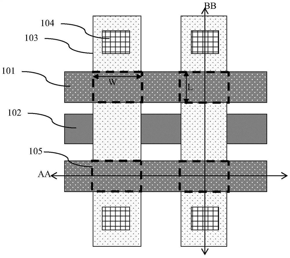
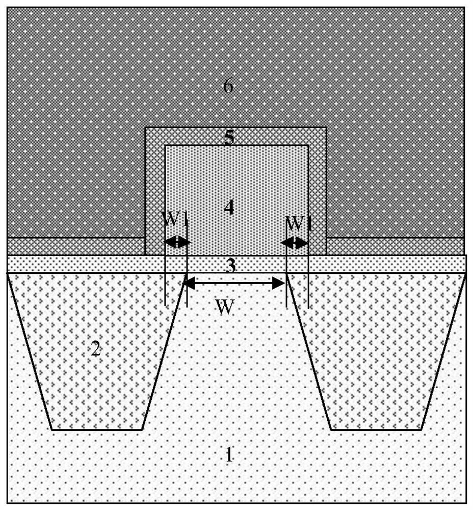
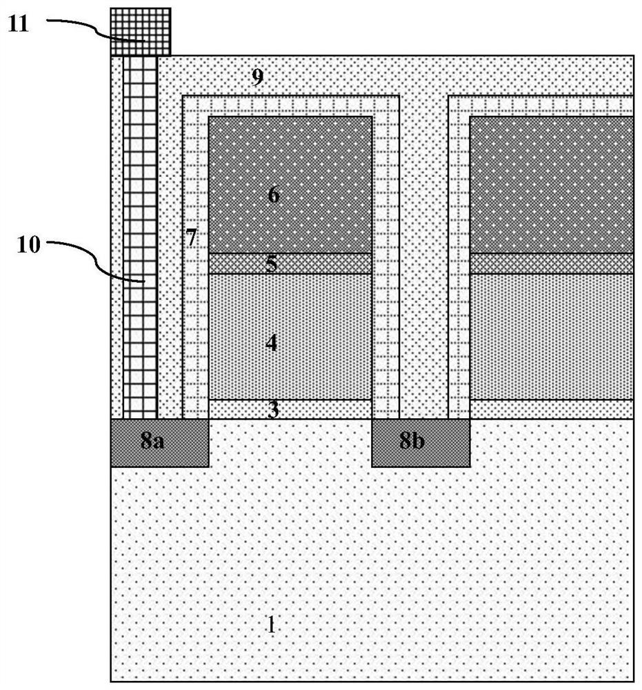
[0038] Such as figure 1 As shown, it is the layout structure of the storage area 202 of the flash memory; as figure 2 shown, is the edge of the existing flash figure 1 Sectional view of line AA in middle; image 3 shown, is the edge of the existing flash figure 1 Sectional view of line BB in middle; Figure 4A Shown is the top view layout of the polysilicon floating gate of the existing flash memory; Figure 4B Shown is a perspective view of a single polysilicon floating gate of an existing flash memory; Figure 4C As shown, it is a three-dimensional view of two adjacent polysilicon floating gates of the existing flash memory; the flash memory in the existing flash memory include...


PUM


Abstract

The invention discloses a flash memory. In a flash memory unit array, active regions isolated by a field oxide layer are included on the surface of a semiconductor substrate, each active region is in a strip structure and arranged in parallel, and a polysilicon floating gate is located in the active region. and isolated by the first gate oxide. In the width direction of the active region, under the condition that the sides of the polysilicon floating gate and the corresponding sides of the active region are photolithographically aligned, the width expansion of the polysilicon floating gate caused by the field oxide layer being etched and consumed will be formed. The two sides of the polysilicon floating gate are provided with a convex-concave structure, and the convex and concave parts of the convex-concave structure are arranged in correspondence with each other so that the side spacing of the polysilicon floating gate is expanded. The invention can reduce the mutual interference between adjacent polysilicon floating gates, which is beneficial to increase the drain voltage and improve the programming speed; it can also increase the coupling rate between the control gate and the floating gate, which is beneficial to further reduce the gate voltage; It is beneficial to further reduce the size of the flash memory unit.

Description

technical field [0001] The invention relates to a semiconductor integrated circuit, in particular to a flash memory (Flash). Background technique [0002] Flash memory has been widely used as the best choice for non-volatile memory applications due to its advantages of high density, low price, and electrical programmability and erasability. At present, flash memory cells are mainly implemented at the 65nm technology node. With the demand for large-capacity flash memory, the number of chips on each silicon wafer will be reduced by using the existing technology nodes. The feature size of high-node technology is smaller, so it can improve the integration of flash memory. At the same time, the maturity of new technology nodes also promotes the production of flash memory cells at high nodes. [0003] In the existing process, theoretically, the width side of the polysilicon floating gate is usually self-aligned with the edge of the active region, but in practice, the width side o...

Claims


Application Information

Patent Timeline
Patent Type & Authority Patents(China)
IPC IPC(8): H01L27/11521H01L27/11524H01L29/423H10B41/30H10B41/35
CPCH01L29/42324H10B41/30H10B41/35
Inventor 田志钟林建
Owner SHANGHAI HUALI MICROELECTRONICS CORP
Features
  • R&D
  • Intellectual Property
  • Life Sciences
  • Materials
  • Tech Scout
  • Unparalleled Data Quality
  • Higher Quality Content
  • 60% Fewer Hallucinations
Learn More