Field local enhancement device based on hybid plasmonic waveguides

A plasmon waveguide and localized technology, which is applied in optical components, light guides, instruments, etc., can solve the problems of unsatisfactory SPP excitation, limitation of the local enhancement effect of the tip field of the double-layer structure, high loss, etc., and achieve Achieve design and integration, break through the limitations of the polarization state, and reduce loss

Active Publication Date: 2018-08-24
NANJING UNIV OF POSTS & TELECOMM +1
View PDF4 Cites 1 Cited by
  • Summary
  • Abstract
  • Description
  • Claims
  • Application Information

AI Technical Summary

Problems solved by technology

[0007] Aiming at the unsatisfactory effect of the SPP excitation of the waveguide with a dielectric-metal double-layer conical structure under the illumination of a radially polarized light source, due to the high loss characteristics of the dielectric-metal plasmon waveguide itself, the tip of the above-mentioned double-layer structure Field-local enhancement effects are limited

Method used


Image

  • Field local enhancement device based on hybid plasmonic waveguides
  • Field local enhancement device based on hybid plasmonic waveguides
  • Field local enhancement device based on hybid plasmonic waveguides

Examples


Embodiment Construction

[0027] Objects, advantages and features of the present invention will be illustrated and explained by the following non-limiting description of preferred embodiments. These embodiments are only typical examples of applying the technical solutions of the present invention, and all technical solutions formed by adopting equivalent replacements or equivalent transformations fall within the protection scope of the present invention.

[0028] The invention discloses a field local enhancement device based on a hybrid plasmon waveguide. The field local enhancement device can locally converge and amplify electromagnetic energy on the nanometer scale, and can locally enhance the field on a limited spatial scale. Specifically, it can be used In the design and integration of nanophotonic devices, new light sources, processing of communication optical fibers, micro-nano sensing and detection and other fields.

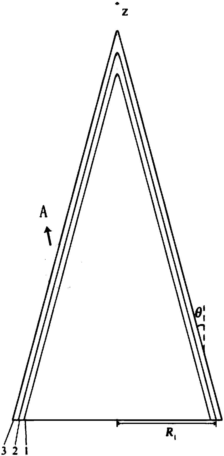
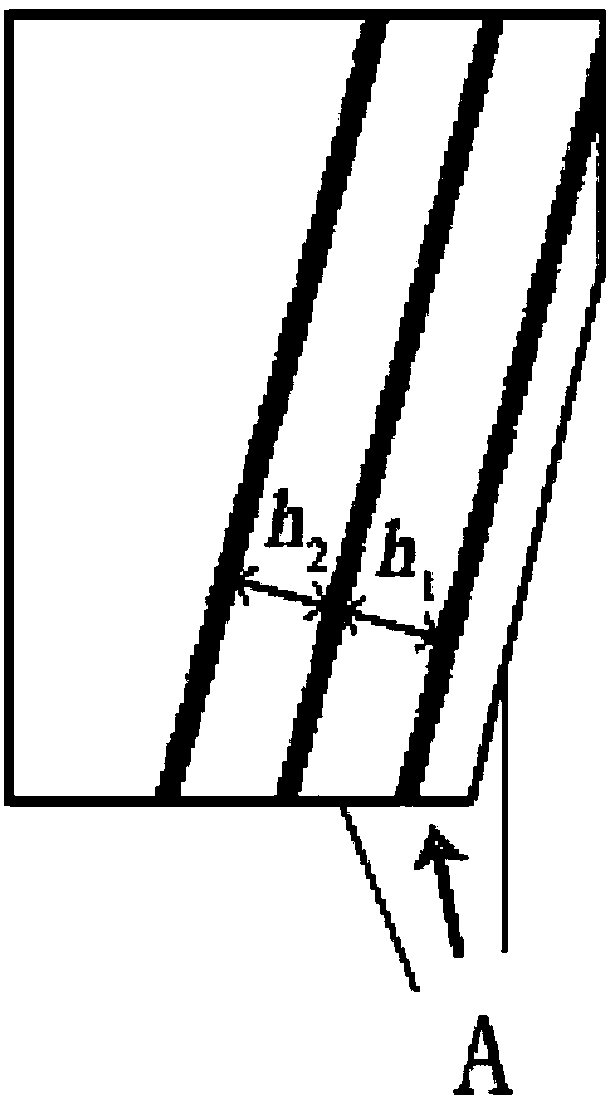
[0029] like figure 1 As shown, the field localized enhancement device based o...


PUM


Abstract

The present invention discloses a field local enhancement device based on hybid plasmonic waveguides. The device comprises three layers of structures consisting of a first layer of structure, a secondlayer of structure and a third layer of structure which form a coaxial conical structure from inside to outside layer by layer, the three layers of structures are respectively medium with a high refractive index, medium with low refractive index and precious metal, when a radially polarized beam vertically enters the structures from the bottom end of a circular cone, the structures can effectively reduce the loss to allow more luminous energy to perform propagation towards the top end, the luminous energy is gathered at the top end and the peak of the circular cone has a high electric field enhancement effect so as to achieve higher focusing performances. The structures can be applied to an ultra-high density integration circuit to have very important application for achieving nanometer photon device design and integration, novel light source, communication fiber processing and micro-nano sensing detection.

Description

technical field [0001] The invention relates to a field local enhancement device based on a hybrid plasmonic waveguide, which can be used in technical fields such as the design and integration of nanophotonic devices, new light sources, processing of communication optical fibers, and micro-nano sensing and detection. Background technique [0002] The requirements of modern information technology for device miniaturization and high integration require the size of unit devices to be smaller and smaller, and the spatial distance of devices to be smaller and smaller, all of which must break through the optical diffraction limit. Based on the basic principles and technical factors of traditional optics, Restricted by the diffraction limit, it is difficult to realize the transmission, processing and related technical applications of related information at the nanoscale level and structure, which cannot meet the needs of the development of science and technology. new technology. ...

Claims


Application Information

Patent Timeline
Patent Type & Authority Applications(China)
IPC IPC(8): G02B5/00G02B6/122G02B6/126
CPCG02B5/008G02B6/1226G02B6/126
Inventor 许吉时楠楠谭朝幻陆昕怡陆云清谌静刘宁
Owner NANJING UNIV OF POSTS & TELECOMM
Why Eureka
Try Eureka