Supercharge Your Innovation With Domain-Expert AI Agents!

A power semiconductor device and a manufacturing method thereof

A technology of power semiconductor and manufacturing method, which is applied in semiconductor devices, semiconductor/solid-state device manufacturing, electrical components, etc., can solve problems such as surface breakdown, and achieve the effect of preventing surface breakdown

Inactive Publication Date: 2018-08-24
INNOSCIENCE (ZHUHAI) TECH CO LTD
View PDF4 Cites 2 Cited by
  • Summary
  • Abstract
  • Description
  • Claims
  • Application Information

AI Technical Summary

Problems solved by technology

[0004] In view of this, the present invention provides a power semiconductor device and its manufacturing method to solve the problem in the prior art that surface breakdown is prone to occur on the curved surface of the gate

Method used


Image

  • A power semiconductor device and a manufacturing method thereof
  • A power semiconductor device and a manufacturing method thereof
  • A power semiconductor device and a manufacturing method thereof

Examples


Embodiment Construction

[0038] The following will clearly and completely describe the technical solutions in the embodiments of the present invention with reference to the accompanying drawings in the embodiments of the present invention. Obviously, the described embodiments are only some, not all, embodiments of the present invention. Based on the embodiments of the present invention, all other embodiments obtained by persons of ordinary skill in the art without making creative efforts belong to the protection scope of the present invention.

[0039] In order to make the above objects, features and advantages of the present invention more comprehensible, the present invention will be further described in detail below in conjunction with the accompanying drawings and specific embodiments.

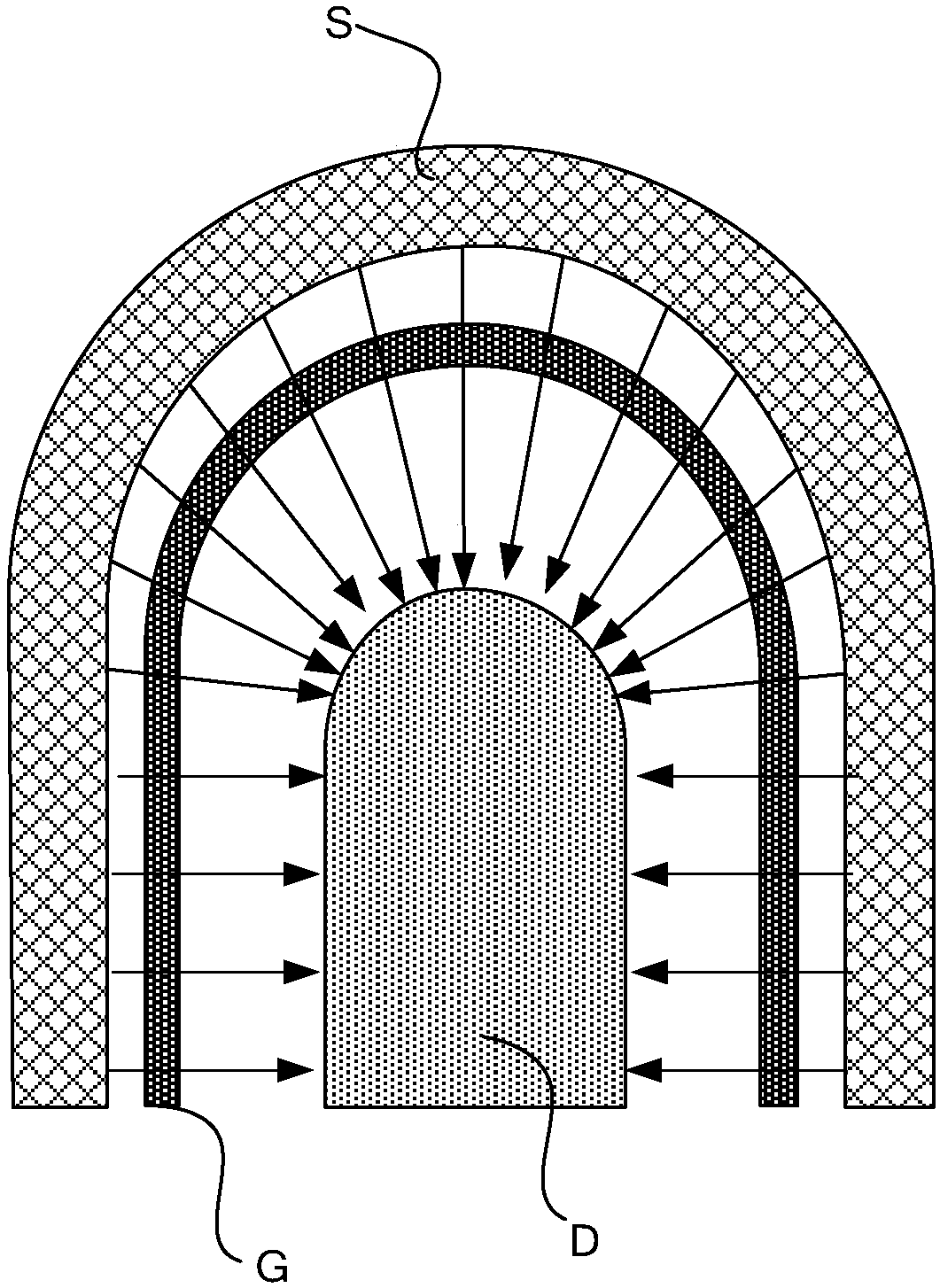
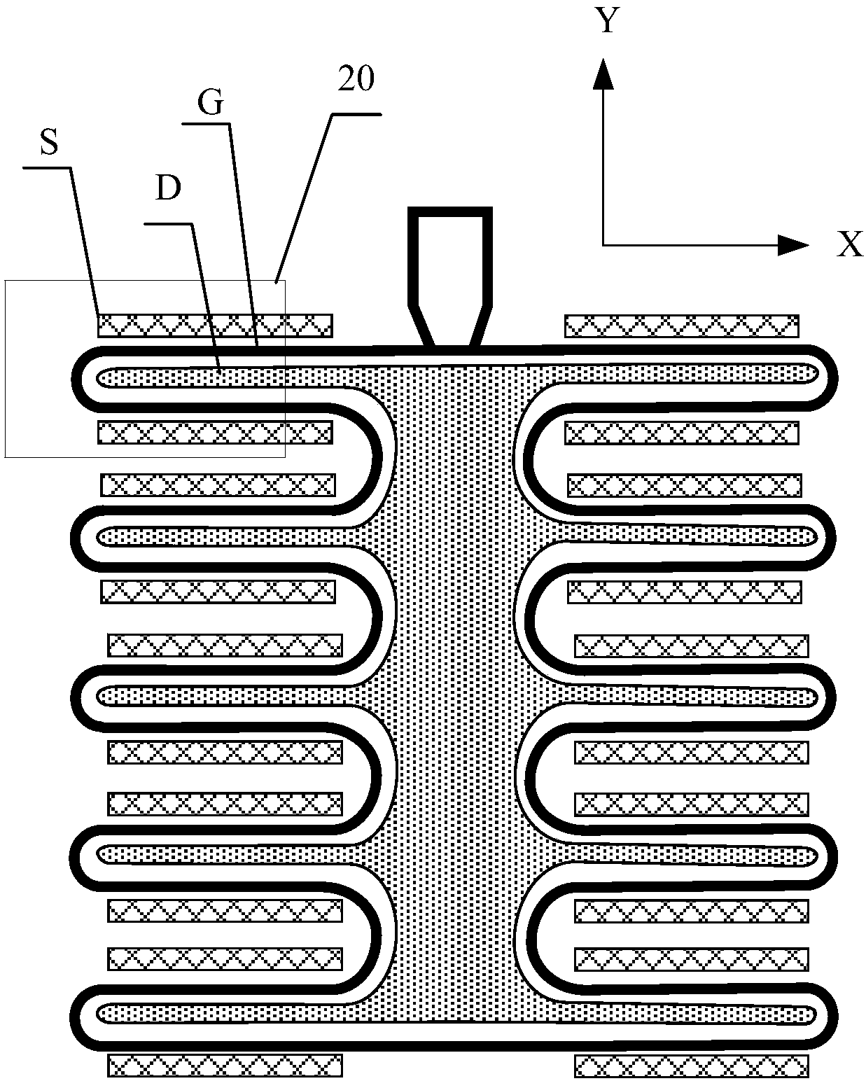
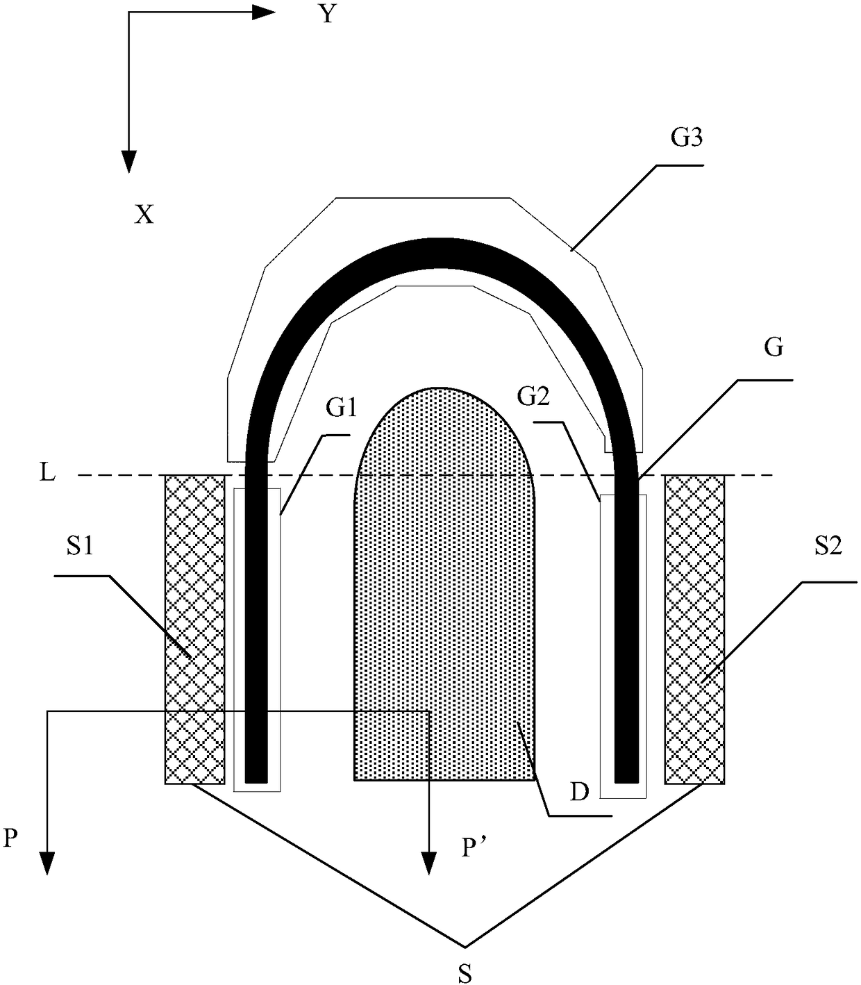
[0040] refer to figure 2 and image 3 , figure 2 A top view of an electrode structure of a power semiconductor device provided by an embodiment of the present invention, image 3 for figure 2 Partial enlarg...


PUM


Abstract

The invention discloses a power semiconductor device and a manufacturing method thereof. The power semiconductor device includes a substrate; a gallium nitride layer is installed on the substrate, thegallium nitride layer includes a grid area, a source electrode area and a drain electrode area; the surface of the grid area is provided with a grid, the surface of the source electrode area is provided with source electrode, and the surface of the drain electrode area is provided with a drain electrode; the grid includes a first grid area and a second grid area which are parallel and relativelyinstalled, the grid also includes a third grid area which is connected with the first grid area and the second grid area, and the third grid area is a curved surface structure; the drain electrode ispositioned between the first grid area and the second grid area; the source electrode includes a first source electrode area and a second source electrode area which are parallel and relatively installed, the first source electrode area and the first grid area are correspondingly installed, and the second source electrode area and the second grid area are correspondingly installed.The problem thatsurface breakdown easily occurs on the curved surface part of the grid in the prior art is solved.

Description

technical field [0001] The present invention relates to the technical field of semiconductor devices, and more specifically, to a power semiconductor device and a manufacturing method thereof. Background technique [0002] Gallium nitride material has the characteristics of large band gap, high saturation drift speed and high temperature resistance, and the heterostructure formed by gallium nitride material has a high two-dimensional electron gas concentration and mobility. Therefore, in the production of high In terms of performance power semiconductor devices, especially in the production of high-speed, low power consumption, and medium and low voltage electronic devices, it has obvious advantages. [0003] refer to figure 1 , figure 1 It is a schematic structural diagram of an existing power semiconductor device, which includes: a thumb-shaped gate G, a source S and a drain D fabricated on a semiconductor substrate. When a voltage is applied to the power semiconductor ...

Claims


Application Information

Patent Timeline
IPC IPC(8): H01L29/778H01L29/417H01L29/423H01L21/335
CPCH01L29/41775H01L29/42316H01L29/66462H01L29/7787
Inventor 李东键金荣善金权济骆薇薇孙在亨
Owner INNOSCIENCE (ZHUHAI) TECH CO LTD
Features
  • R&D
  • Intellectual Property
  • Life Sciences
  • Materials
  • Tech Scout
  • Unparalleled Data Quality
  • Higher Quality Content
  • 60% Fewer Hallucinations
Learn More