Micro three-dimensionak device and preparation method and application thereof

A technology of three-dimensional devices, applied in the field of micro-three-dimensional devices and their preparation, can solve the problems that micro-devices cannot achieve high-precision miniaturization and three-dimensionalization, high manufacturing costs, and reduced manufacturing costs, etc., to achieve mass production and low cost Effect

Active Publication Date: 2018-09-04
INST OF CHEM CHINESE ACAD OF SCI
View PDF9 Cites 2 Cited by
  • Summary
  • Abstract
  • Description
  • Claims
  • Application Information

AI Technical Summary

Problems solved by technology

[0004] The purpose of the present invention is to provide micro-stereoscopic devices and their preparation methods and applications, which can meet Miniaturization and three-dimensional high-precision requirements, and the preparation cost is greatly reduced

Method used


Image

  • Micro three-dimensionak device and preparation method and application thereof
  • Micro three-dimensionak device and preparation method and application thereof
  • Micro three-dimensionak device and preparation method and application thereof

Examples


preparation example Construction

[0027] The first aspect of the present invention provides a method for preparing a miniature three-dimensional device, wherein the method includes the following steps:

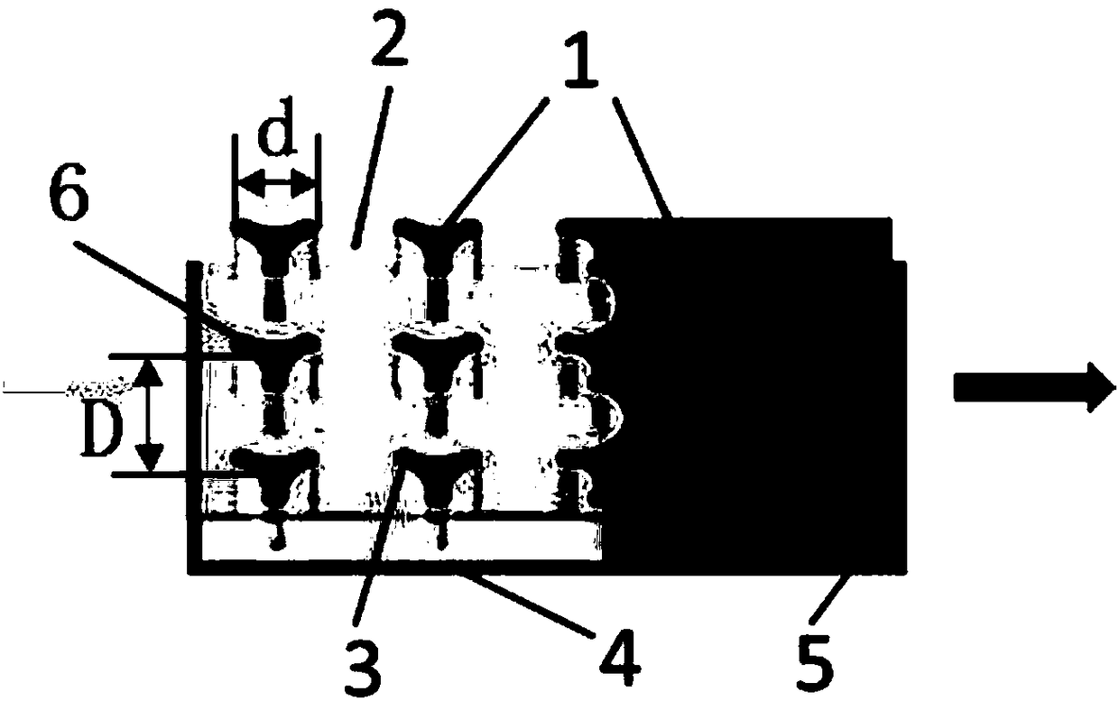
[0028] (A) Prepare a substrate 4 having a plurality of patterned structural units 3 and having hydrophilic properties, wherein the ratio of the distance D between two adjacent patterned structural units 3 to the size d of the patterned structural units 3 is not equal to less than 2;

[0029] (B) Assembling the substrate 4 with a substrate 5 with a flat surface to obtain a microfluidic device with an interlayer;

[0030] (C) Inject the first solution 1 containing the first functional material and the first solvent into the microfluidic device and fill the interlayer, then pass the gas 2 to evaporate the first solvent, and form the first functional material on the surface of the patterned structural unit 3 The three-dimensional self-assembled structure of the obtained micro-stereoscopic device containing a sing...

Embodiment 1

[0079] (1) Preparation of substrates with multiple patterned structural units and hydrophilic properties

[0080] Select a square silicon substrate with a side length of 5 inches (such as figure 2 As shown in the label 4 in ), adopt the method of conventional mask optical etching to etch the raised cylindrical silicon pillars (basic units, such as figure 2 6), each circular silicon pillar is 20 μm in height and 10 μm in diameter, and the patterned structural unit (such as figure 2 3) is a triangle composed of three cylinders, the size d of the patterned structural unit is 50 μm, and the distance D between two adjacent patterned structural units is 110 μm.

[0081] Then the substrate was treated with a power of 150W for 300s in an oxygen plasma treatment apparatus to perform hydrophilic treatment.

[0082] (2) Preparation of a microfluidic device with an interlayer

[0083] Place the silicon wafer with multiple patterned structural units horizontally, and then cover it wi...

Embodiment 2

[0092] (1) Preparation of substrates with multiple patterned structural units and hydrophilic properties

[0093] Select a circular silicon wafer substrate with a diameter of 5 inches, and use a conventional mask optical etching method to etch cylindrical silicon pillars on the surface of the silicon wafer. Each circular silicon pillar has a height of 30 μm and a diameter of 15 μm. The patterned structural unit is a triangle composed of three cylinders, the size d of the patterned structural unit is 15 μm, and the distance D between two adjacent patterned structural units is 180 μm.

[0094] Then the substrate was treated with a power of 150W for 300s in an oxygen plasma treatment apparatus to perform hydrophilic treatment.

[0095] (2) Preparation of a microfluidic device with an interlayer

[0096] Place the silicon wafer with multiple patterned structural units horizontally, and then cover it with a glass sheet with a flat surface. The glass sheet has four holes with a dia...


PUM

PropertyMeasurementUnit
viscosityaaaaaaaaaa
heightaaaaaaaaaa
diameteraaaaaaaaaa

Abstract

The invention relates to the material field, and discloses a micro three-dimensional device and a preparation method and application thereof. The preparation method of the micro three-dimensional device comprises the following steps that 1, a substrate which is provided with multiple patterned structure units and has the hydrophilic nature is prepared, wherein the ratio of the distance D between every two adjacent patterned structure units to the size d of the patterned structure units is no less than 2; 2, the substrate and a base material with the flat surface are assembled to obtain a microfluid device with interlayers; and 3, a first solution containing a first function material and first solvent is injected into the microfluid device to enable the interlayers to be filled with the first solution, then gas is introduced to evaporate the first solvent, three-dimensional self-assembled structures of the first function material are formed on the surfaces of the patterned structure units, and then a micro three-dimensional device containing a single layer of function material is obtained. According to the micro three-dimensional device, the high-precision requirements on miniaturization and three-dimension can be met, and the preparation cost is greatly reduced.

Description

technical field [0001] The invention relates to the field of materials, in particular to a micro three-dimensional device and a preparation method and application thereof. Background technique [0002] The properties of functional materials in terms of light, electricity, force, heat, magnetism, and sound make them have great application prospects in industrial applications. With the rapid development of functional material synthesis technology, the limitation of its popularization and application in production and life is more and more apparent in the preparation technology of functional devices. Functional material assembly technology acts as a bridge connecting functional materials and functional devices, and its bottom-up preparation method has great development advantages of cleanness, low cost, and simple operation. [0003] With the large demand for wearable and portable devices in the society, the miniaturization and three-dimensionalization of devices are an import...

Claims


Application Information

Patent Timeline
Patent Type & Authority Applications(China)
IPC IPC(8): B81C1/00B81B1/00
CPCB81B1/002B81C1/00119
Inventor 黄占东苏萌李正蔡哲仁宋延林
Owner INST OF CHEM CHINESE ACAD OF SCI
Why Eureka
Try Eureka