IGBT apparatus provided with internal JFET structure

A device and gate structure technology, applied in the field of power semiconductor devices, can solve the problems of increased device turn-off loss, low discharge efficiency, affecting gate control capability, etc. Withstand voltage and working reliability, the effect of avoiding short-circuit failure phenomenon

Active Publication Date: 2018-09-04
UNIV OF ELECTRONICS SCI & TECH OF CHINA
View PDF6 Cites 5 Cited by
  • Summary
  • Abstract
  • Description
  • Claims
  • Application Information

AI Technical Summary

Problems solved by technology

However, the FP region between the trench gates stores excess holes during forward conduction, which will introduce negative gate capacitance effect to generate displacement current in the gate, which affects the gate control ability; it takes time for the hole current to discharge when it is turned off, making the device The turn-off loss increases
At the same time, if the holes cannot be extracted from the FP region in time during the turn-off process, the leakage current after turn-off will be too large, which will induce delayed failure and reduce the turn-off capability of the device.
The existing solution provides a discharge path for holes in the FP region when it is turned off by introducing clamping diodes and diffusion resistors, but it exposes problems such as low discharge efficiency and damaged device breakdown voltage.

Method used


Image

  • IGBT apparatus provided with internal JFET structure
  • IGBT apparatus provided with internal JFET structure
  • IGBT apparatus provided with internal JFET structure

Examples


Embodiment

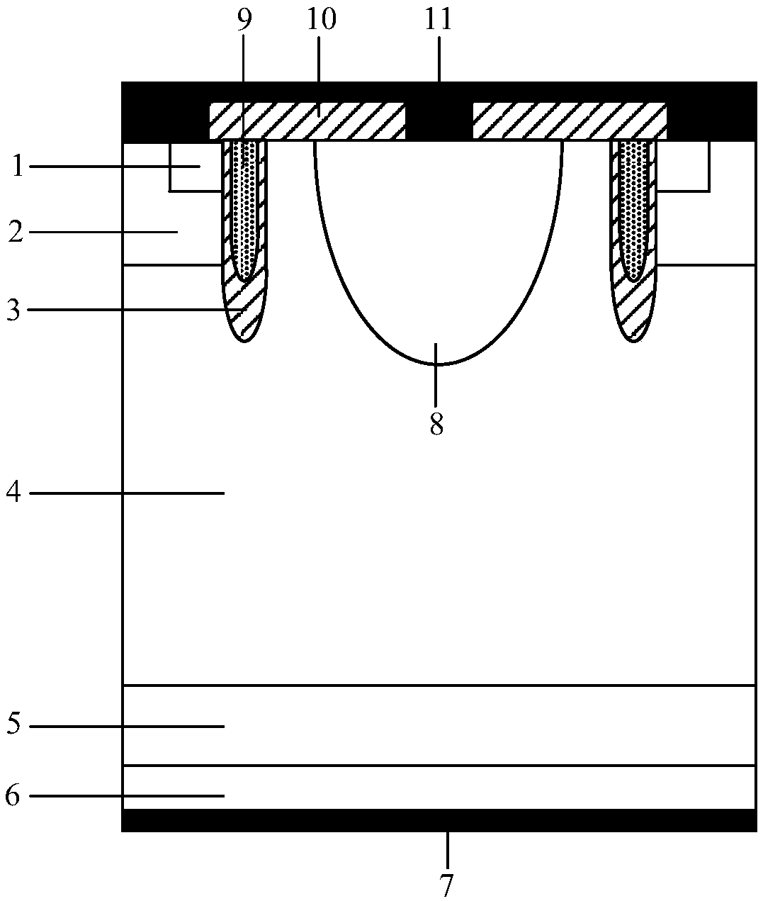
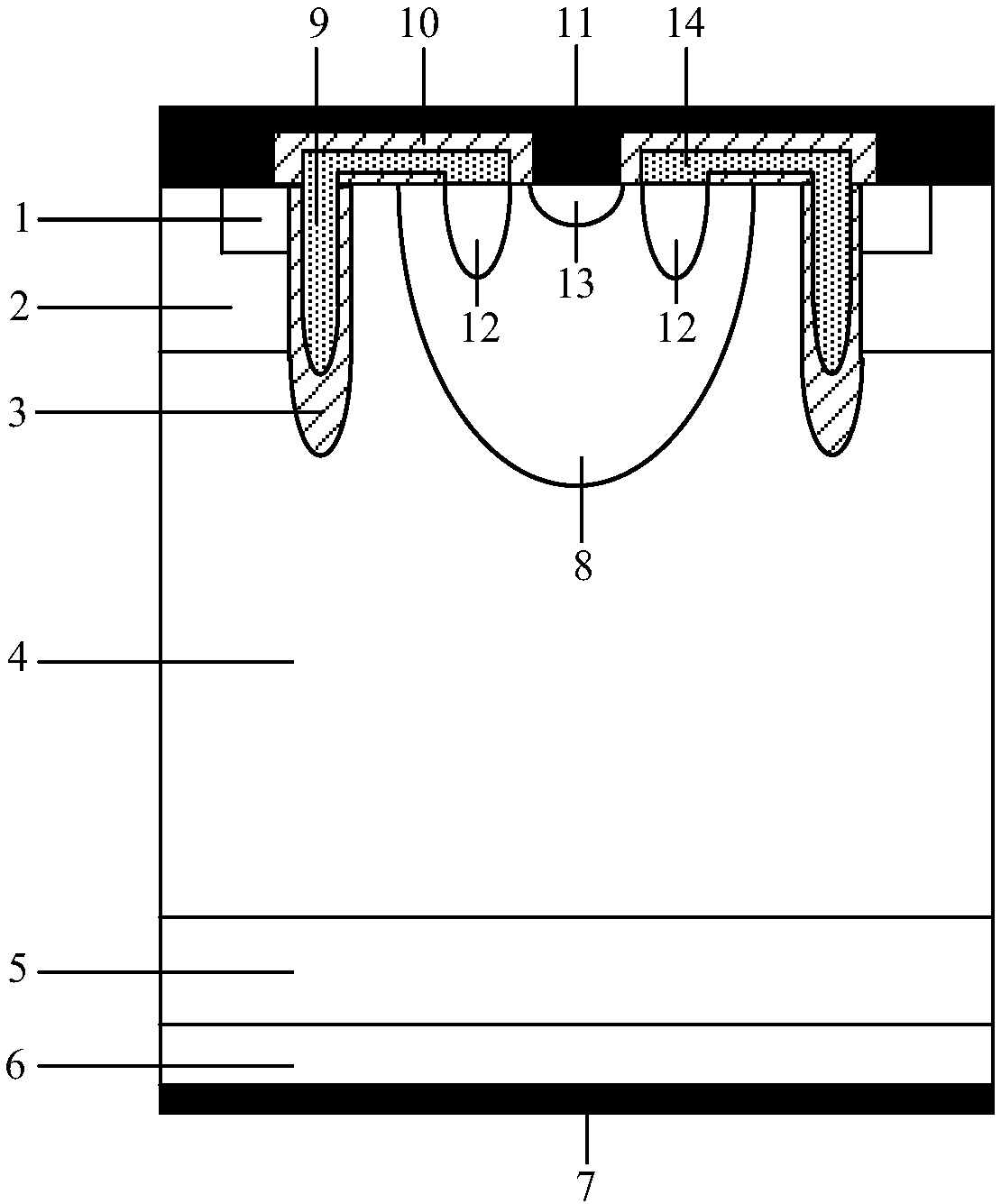
[0031] An IGBT device with a built-in JFET structure such as figure 2As shown, its cellular structure includes a metal collector 7, a first conductivity type semiconductor collector region 6, a second conductivity type semiconductor buffer layer 5, a second conductivity type semiconductor drift region 4, and a metal emitter stacked sequentially from bottom to top. Pole 11; the top layer of the second conductivity type semiconductor drift region 4 has a first conductivity type semiconductor body region 8, a first conductivity type semiconductor base region 2, a second conductivity type semiconductor emitter region 1 and a gate structure; the second conductivity type semiconductor A semiconductor body region 8 of a conductivity type is located in the middle region of the top layer of the semiconductor drift region 4 of the second conductivity type; the semiconductor base region 2 of the first conductivity type is respectively located in regions on both sides of the top layer of ...


PUM


Abstract

The invention relates to an IGBT apparatus provided with an internal JFET structure and belongs to the technical field of power semiconductor apparatuses. According to the IGBT apparatus structure, byintroducing a JEFT region in a body region of a conventional grate IGBT, the JFET region is equivalent to a variable resistor, a hole is stored when the apparatus is conducted forward and a quick releasing circuit is provided for the hole in forward blockage, so that the saturated conducting pressure drop and cut-off loss of the apparatus are reduced, the short-circuit failure phenomenon after the apparatus is cut off is avoided, and the cut-off ability of the apparatus is improved; moreover, a connecting bridge connecting the grate structure and the JFET region plays a field plate role whenthe apparatus is blocked forwardly, so that the electric field peak on the surface of the lower region of the connecting bridge is reduced effectively, and the voltage-resistant and operational reliability of the apparatus is improved. The IGBT apparatus provided with the internal JFET structure is compatible to an existing high voltage IGBT apparatus manufacturing process, so that industrialization is achieved favorably.

Description

technical field [0001] The invention belongs to the technical field of power semiconductor devices, and in particular relates to an IGBT device with a built-in JFET structure. Background technique [0002] With the rapid development of rail transit, smart grid, green energy and other fields, insulated gate bipolar transistor (Insulated Gate Bipolar Transistor, IGBT) has simple gate control, high input impedance, fast switching speed, high current density, saturation voltage It has become one of the mainstream power switching devices in the field of medium and high power power electronics; at the same time, it will continue to develop in the direction of high voltage, high current, high operating temperature and high reliability. The application of IGBT devices in high-voltage applications, especially in the process of motor driving, will experience a short circuit at both ends of the device; the device will be turned on when the load is short-circuited, resulting in a short-...

Claims


Application Information

Patent Timeline
Patent Type & Authority Applications(China)
IPC IPC(8): H01L29/739H01L29/40
CPCH01L29/402H01L29/7397
Inventor 李泽宏彭鑫赵倩杨洋张金平高巍任敏张波
Owner UNIV OF ELECTRONICS SCI & TECH OF CHINA
Why Eureka
Try Eureka