

Semiconductor device
A semiconductor and conductor layer technology, applied in the direction of semiconductor devices, semiconductor/solid-state device parts, amplifiers with semiconductor devices/discharge tubes, etc., can solve the problem of increasing the chip area and achieve the effect of increasing the operating frequency
- Summary
- Abstract
- Description
- Claims
- Application Information
AI Technical Summary
Problems solved by technology
Method used
Image

Examples
no. 1 Embodiment
[0123] refer to Figures 1A to 5 , the semiconductor device according to the first embodiment will be described.
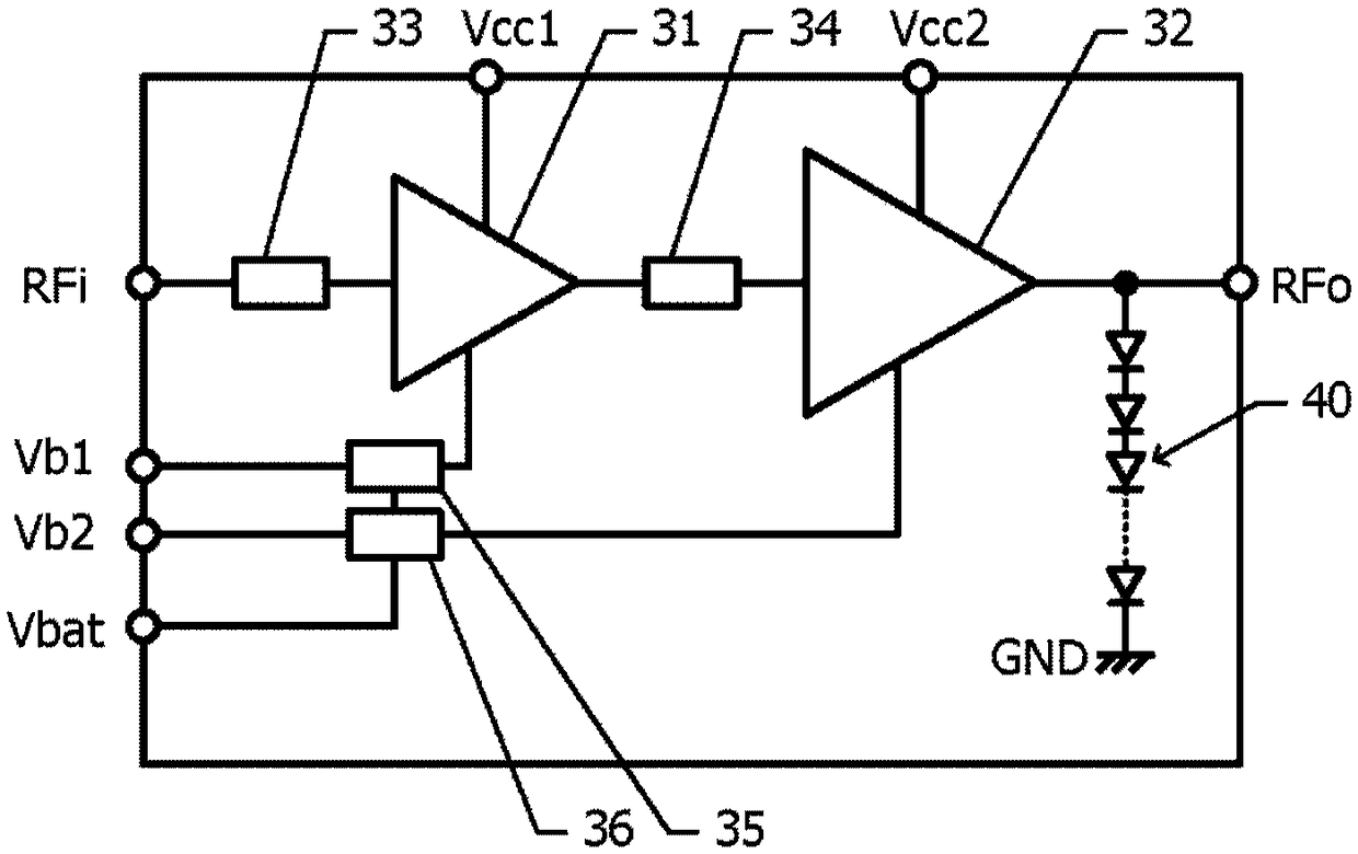
[0124] Figure 1A It is a block diagram of a power amplifier module incorporating the semiconductor device based on this embodiment. The input signal input from the high-frequency input terminal RFi is input to the input stage amplifier circuit 31 via the matching circuit 33 . The signal amplified by the input stage amplifier circuit 31 is input to the output stage amplifier circuit 32 via the matching circuit 34 . The output signal amplified by the output stage amplifier circuit 32 is output from the high frequency output terminal RFo.
[0125] A bias voltage is applied to the bias circuits 35 and 36 from the bias voltage terminal Vbat. Based on the signal input from the bias control terminal Vb1 , the bias circuit 35 supplies a bias current to the input stage amplifier circuit 31 . The bias circuit 36 supplies a bias current to the output stage amplifier c...
no. 2 Embodiment
[0179] Next, refer to Image 6 and Figure 7 A semiconductor device based on the second embodiment will be described. Hereinafter, descriptions of the configurations common to those of the semiconductor device according to the first embodiment will be omitted.
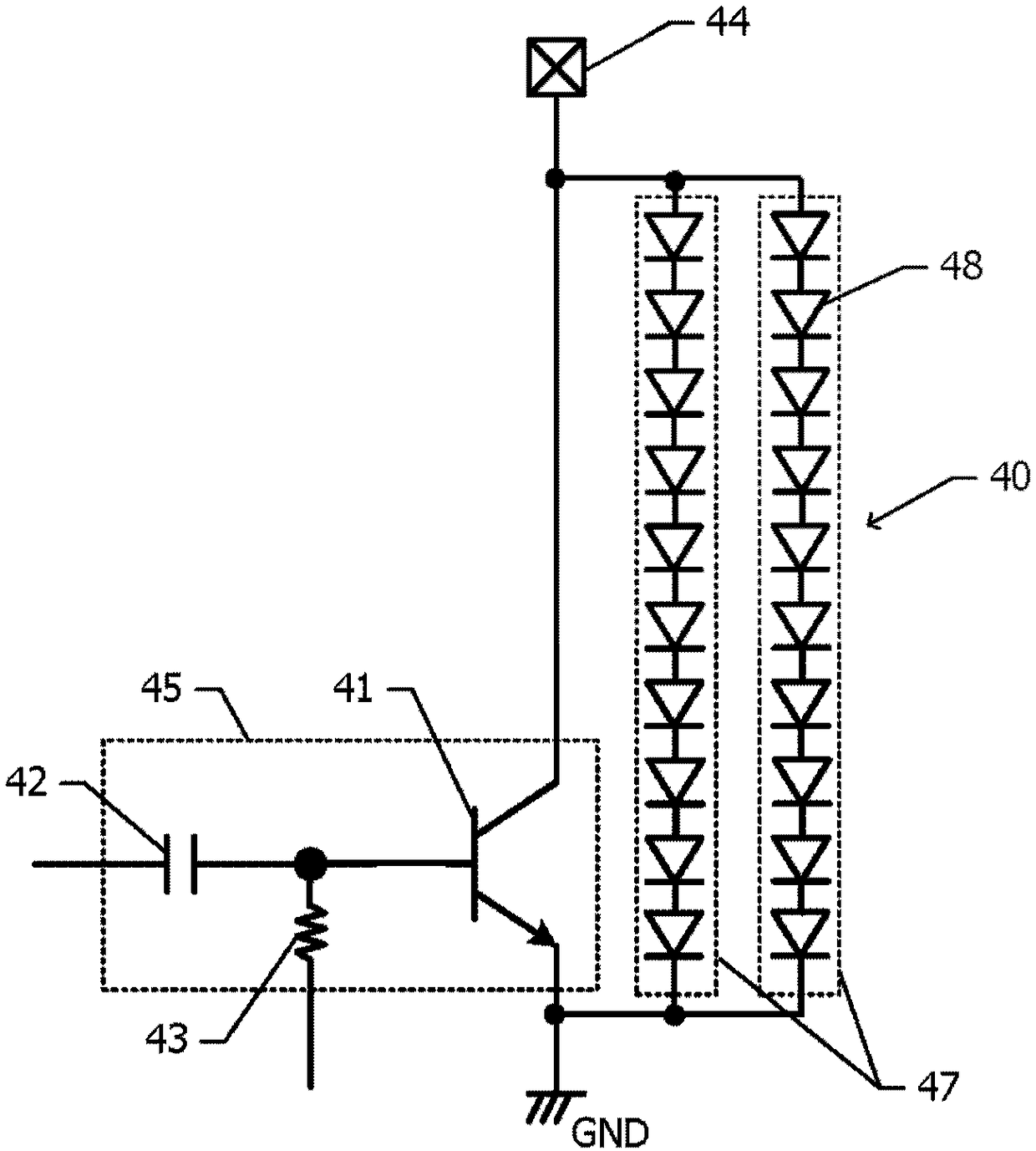
[0180] Image 6 is the output stage amplifier circuit 32 ( Figure 1A ) and the equivalent circuit diagram of the protection circuit 40 . In the first embodiment, the protection circuit 40 is constituted by two diode series circuits 47, but in the second embodiment, the protection circuit 40 is constituted by one diode series circuit.
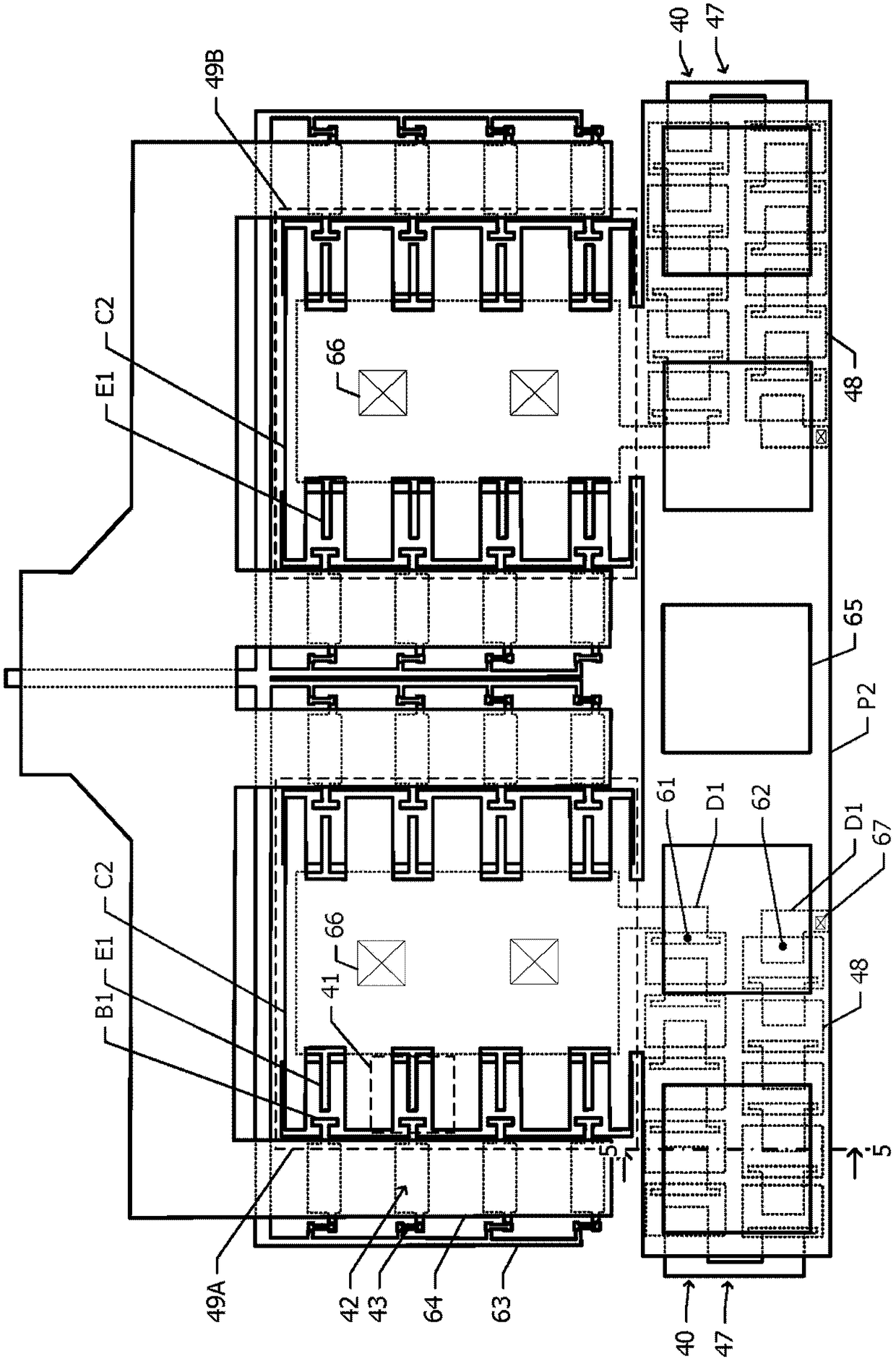
[0181] Figure 7 This is a plan view of the semiconductor device according to the second embodiment. In the first embodiment, as figure 2 As shown, a diode series circuit 47 is connected to the emitter wiring E1 of the first HBT cell block 49A and the emitter wiring E1 of the second HBT cell block 49B, respectively. In contrast, in the second embodiment, the protection circuit 4...
no. 3 Embodiment
[0187] Next, refer to Figure 8 A semiconductor device based on the third embodiment will be described. Hereinafter, descriptions of the configurations common to those of the semiconductor device according to the second embodiment will be omitted.
[0188] Figure 8 This is a plan view of the semiconductor device according to the third embodiment. In the second embodiment, the protection circuit 40 ( Figure 7 ) of the protection diodes 48 are arranged along one straight line. In the third embodiment, the diode array composed of the plurality of protection diodes 48 constituting the protection circuit 40 is folded back halfway. The foldback location does not have to be the middle of the diode column.
[0189] In the third embodiment, the protection circuit 40 also overlaps with the pad conductor layer P2. Therefore, the same effects as those of the second embodiment can be obtained. Furthermore, since the diode row can be folded back at an arbitrary position, the degree...
PUM
 Abstract
Description
Claims
Application Information