A voltage-resistant bipolar transistor and its manufacturing method
A bipolar transistor and withstand voltage technology, which is applied in semiconductor/solid-state device manufacturing, semiconductor devices, electrical components, etc., can solve the problems of low withstand voltage and weak resistance, so as to increase the breakdown voltage and increase BE Junction area, overcoming the effect of larger BE junction current density
- Summary
- Abstract
- Description
- Claims
- Application Information
AI Technical Summary
Problems solved by technology
Method used
Image
Examples
Embodiment 1
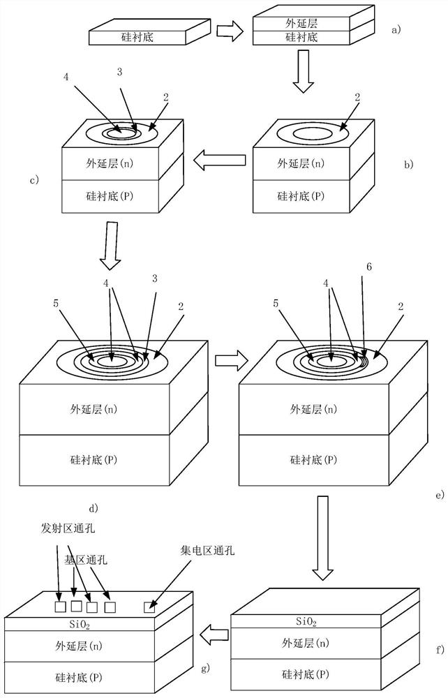
[0029] Step 1: Select the substrate.
[0030] First, a lightly doped P-type silicon is selected as the initial material to be used as the substrate;
[0031] Step 2: growing the epitaxial layer.
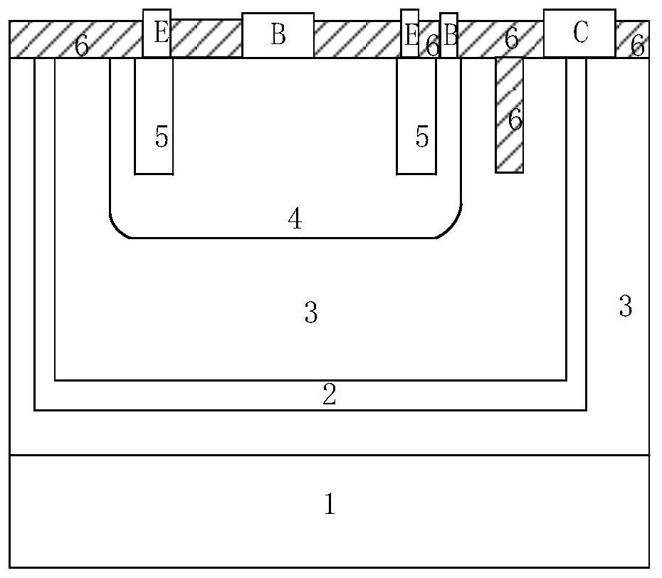
[0032] An N-type doped low-concentration epitaxial layer 3 is formed on the top of the silicon substrate 1 by chemical vapor deposition under vacuum conditions, and the doping concentration is on the order of 8e15cm -3 , the doping element is arsenic, and the thickness is 2um-10um. The epitaxial layer acts as the collector area of the transistor;
[0033] Step 3: Make a heavily doped collector region.
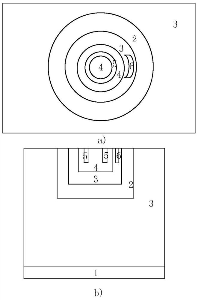
[0034] A layer of silicon dioxide is grown on the surface of the epitaxial layer by a thermal oxidation process, and then the photoresist is spin-coated, exposed by a photolithography machine, and a cylindrical pattern of a heavily doped region is made, namely figure 1 In the region 2 shown in a), etch out the heavily doped collector region that needs ion implantation, and selec...
Embodiment 2
[0051] Step 1: Select the substrate.
[0052] First, a lightly doped P-type silicon is selected as the initial material to be used as the substrate;
[0053] Step 2: growing the epitaxial layer.
[0054] An N-type doped low-concentration epitaxial layer 3 is formed on the top of the silicon substrate 1 by chemical vapor deposition under vacuum conditions, and the doping concentration is on the order of 8e15cm -3 , the doping element is phosphorus, and the thickness is 2um-10um. This epitaxial layer acts as the collector region of the transistor.
[0055] Steps 3-7 are the same as in Example 1.
Embodiment 3
[0057] Step 1-3 is the same as embodiment 1 or 2;
[0058] Step 4: Make the trench.
[0059] A thin layer of silicon dioxide is grown on the surface of the epitaxial layer by a thermal oxidation process, and then the photoresist is spin-coated, exposed by a photolithography machine, and the pattern that needs to be oxidized is made, and etched away by dry etching technology SiO2 and epitaxial layers, thus forming two bilaterally symmetrical SiO 2 trenches, respectively, for the first SiO 2 Trench and second SiO 2 Trench, the depth of which is the same as the junction depth of the emitter region; these two trenches can suppress the lateral breakdown between the collector region and the base region; remove residual silicon dioxide and photoresist.
[0060] Cylindrical heavily doped collector, SiO 2 The trench and the base region are not in contact with each other, and are separated by a low-concentration collector region, that is, separated by an N-type doped low-concentrati...
PUM
 Abstract
Description
Claims
Application Information


