Withstand voltage bipolar transistor and manufacturing method thereof

A bipolar transistor and withstand voltage technology, which is applied in semiconductor/solid-state device manufacturing, semiconductor devices, electrical components, etc., can solve the problems of weak resistance and low withstand voltage value, so as to increase the breakdown voltage value and increase BE Junction area, overcoming the effect of larger BE junction current density

Active Publication Date: 2018-09-11
XI'AN UNIVERSITY OF ARCHITECTURE AND TECHNOLOGY
View PDF7 Cites 3 Cited by
  • Summary
  • Abstract
  • Description
  • Claims
  • Application Information

AI Technical Summary

Problems solved by technology

[0004] The purpose of the present invention is to solve the problem of weak resistance and low withstand voltage value of the existing bipolar transistor in the EMP environment, and propose a withstand voltage bipolar transistor and its manufacturing method, by increasing the contact area of ​​the PN junction and reducing the The above current collector effect, and then improve the withstand voltage characteristics of the collector junction, so as to achieve the purpose of improving the reliability of the transistor as a whole

Method used


Image

  • Withstand voltage bipolar transistor and manufacturing method thereof
  • Withstand voltage bipolar transistor and manufacturing method thereof
  • Withstand voltage bipolar transistor and manufacturing method thereof

Examples


Embodiment 1

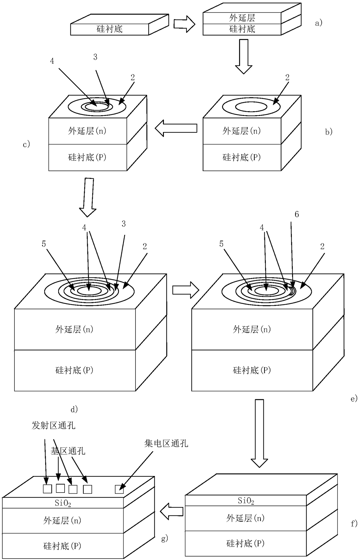
[0029] Step 1: Select the substrate.

[0030] First, a lightly doped P-type silicon is selected as the initial material to be used as the substrate;

[0031] Step 2: growing the epitaxial layer.

[0032] An N-type doped low-concentration epitaxial layer 3 is formed on the top of the silicon substrate 1 by chemical vapor deposition under vacuum conditions, and the doping concentration is on the order of 8e15cm -3 , the doping element is arsenic, and the thickness is 2um-10um. The epitaxial layer acts as the collector area of ​​the transistor;

[0033] Step 3: Make a heavily doped collector region.

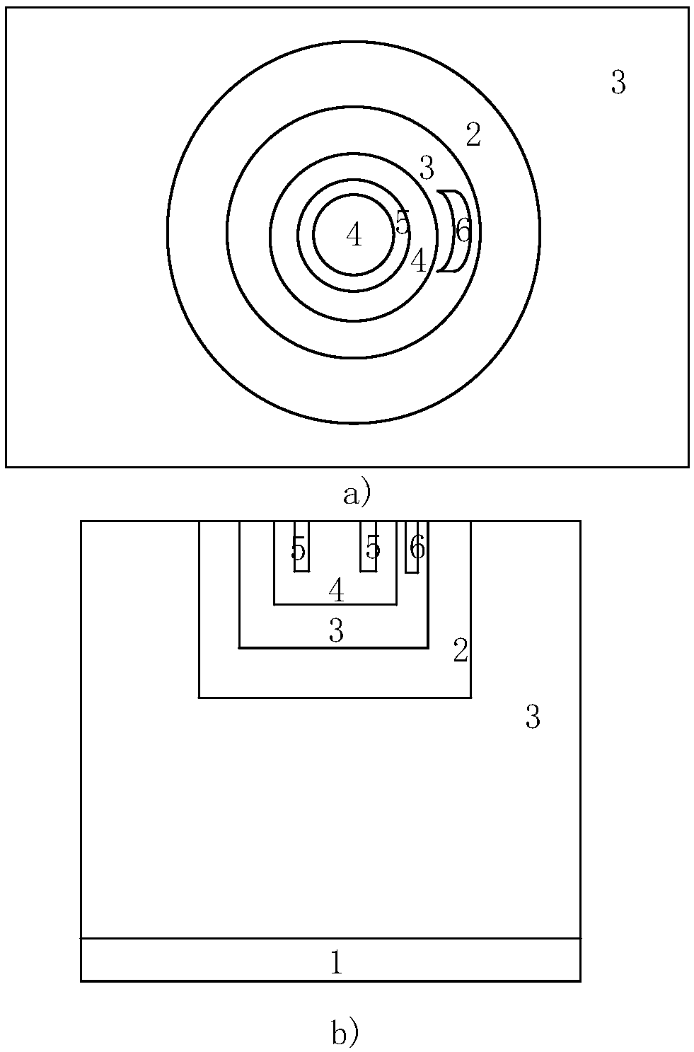
[0034] A layer of silicon dioxide is grown on the surface of the epitaxial layer by a thermal oxidation process, and then the photoresist is spin-coated, exposed by a photolithography machine, and a cylindrical pattern of a heavily doped region is made, namely figure 1 In the region 2 shown in a), etch out the heavily doped collector region that requires ion implantation, and se...

Embodiment 2

[0051] Step 1: Select the substrate.

[0052] First, a lightly doped P-type silicon is selected as the initial material to be used as the substrate;

[0053] Step 2: growing the epitaxial layer.

[0054] An N-type doped low-concentration epitaxial layer 3 is formed on the top of the silicon substrate 1 by chemical vapor deposition under vacuum conditions, and the doping concentration is on the order of 8e15cm -3 , the doping element is phosphorus, and the thickness is 2um-10um. This epitaxial layer acts as the collector region of the transistor.

[0055] Steps 3-7 are the same as in Example 1.

Embodiment 3

[0057] Step 1-3 is the same as embodiment 1 or 2;

[0058] Step 4: Make the trench.

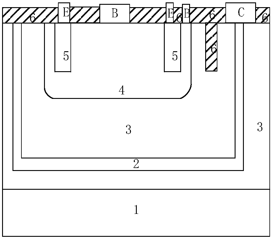
[0059] A thin layer of silicon dioxide is grown on the surface of the epitaxial layer by a thermal oxidation process, and then the photoresist is spin-coated, exposed by a photolithography machine, and the pattern that needs to be oxidized is made, and etched away by dry etching technology SiO2 and epitaxial layers, thus forming two bilaterally symmetrical SiO 2 trenches, respectively, for the first SiO 2 Trench and second SiO 2 Trench, the depth of which is the same as the junction depth of the emitter region; these two trenches can suppress the lateral breakdown between the collector region and the base region; remove residual silicon dioxide and photoresist.

[0060] Cylindrical heavily doped collector, SiO 2 The trench and the base region are not in contact with each other, and are separated by a low-concentration collector region, that is, separated by an N-type doped low-concentrati...


PUM


Abstract

The invention discloses a withstand voltage bipolar transistor and manufacturing method thereof, and mainly solves the problem that an existing bipolar transistor is low in resistance and has a low withstand voltage value in an EMP environment. The withstand voltage bipolar transistor includes a substrate (1), a heavily-doped collector region (2), an epitaxial layer (3), a base region (4), an emitter region (5), a SiO2 layer (6), a SiO2 trench and a through hole. The heavily-doped collector region is cylindric, is located in the epitaxial layer, and divides the epitaxial layer into two parts,i.e., an in-cylinder epitaxial layer and outside-cylinder epitaxial layer; the in-cylinder epitaxial layer includes the cylindrical base region and the SiO2 trench which has the same junction depth asthe emitter region; and the base region includes the emitter region which in a circular ring shape. The method provided by the invention effectively reduces a current crowding effect on an emitter junction, thereby improving a withstand voltage characteristic of a collector junction; and solves the problem in the prior art that the overall withstand voltage characteristic of the transistor cannotbe improved only by protection of a specific input and output end, and achieves the purpose of improving transistor reliability on the whole.

Description

technical field [0001] The invention belongs to the technical field of semiconductor devices, in particular to an NPN type voltage-resistant bipolar transistor, which can be used to make power devices, digital logic circuit devices or power electronic devices and the like. Background technique [0002] A bipolar transistor includes a base region, an emitter region, and a collector region. When a small amount of current is injected into the base region of the transistor biased in the amplification region, the base region current will be amplified between the emitter region and the collector region. This is the transistor amplification effect. With the development of pulse power technology and the improvement of microelectronics technology, high-frequency power transistor devices are widely used in communication systems. However, in real conditions, high-power microwaves at various frequencies generated by various pulse power generating devices make The current electromagneti...

Claims


Application Information

Patent Timeline
Patent Type & Authority Applications(China)
IPC IPC(8): H01L29/735H01L29/08H01L21/331
CPCH01L29/0808H01L29/6625H01L29/735
Inventor 樊庆扬张文柱卫铭斐
Owner XI'AN UNIVERSITY OF ARCHITECTURE AND TECHNOLOGY
Why Eureka
Try Eureka