Multifunction near-field optical probe based on Plasmon nanonail structure

A plasmon and near-field optical technology, which is applied in the field of near-field microscopy and nanomaterials, and can solve problems such as single probe

Inactive Publication Date: 2018-09-14
SOUTHEAST UNIV
View PDF0 Cites 16 Cited by
  • Summary
  • Abstract
  • Description
  • Claims
  • Application Information

AI Technical Summary

Problems solved by technology

[0006] On the other hand, today's probes

Method used


Image

  • Multifunction near-field optical probe based on Plasmon nanonail structure
  • Multifunction near-field optical probe based on Plasmon nanonail structure

Examples


Embodiment

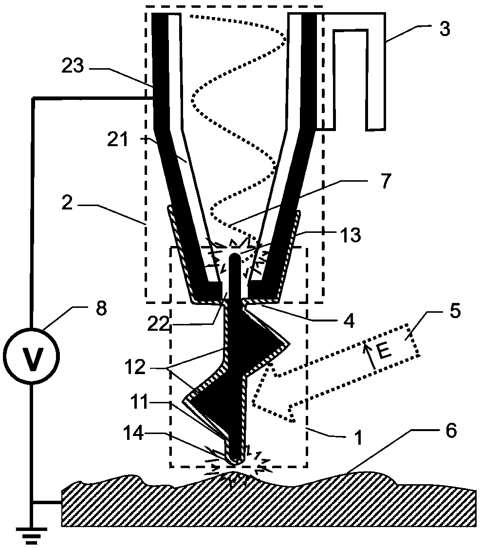
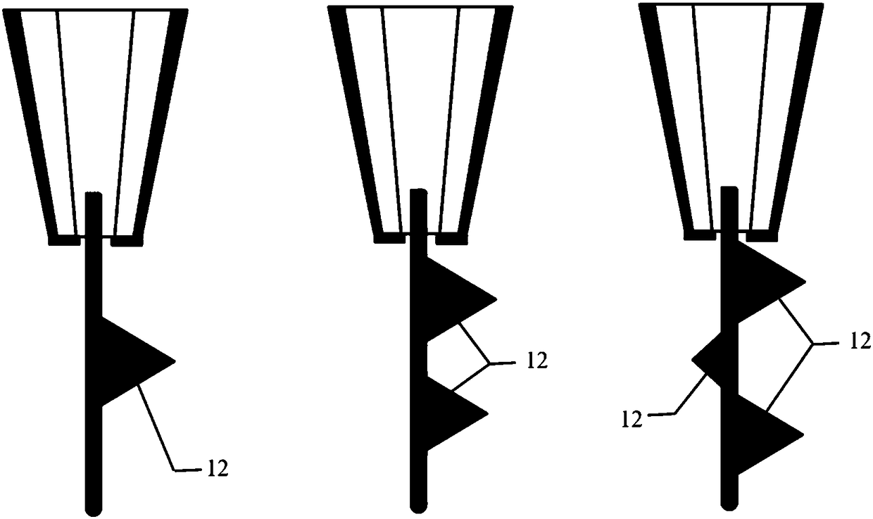
[0044] The structure of the multifunctional near-field optical probe with nanonail structure is as follows: figure 1 As shown, wherein the silver nanonail tip 1, it is made up of the silver triangular plate 12 that two side lengths are 150nm and 200nm respectively on the silver nanowire 11 that diameter is 10nm and length is 5 μ m; Tapered optical fiber 2, it is made up of optical fiber 21 and surface-plated aluminum film 23 constitute; tuning fork 3, which is rigidly connected with the tapered optical fiber. One end 13 of the silver nanonail is inserted into the opening 22) of the tapered probe, wherein the opening is 50nm, and the insertion depth is 100nm. At the same time, the tip of the nano-nail is connected to the aluminum film through a single-layer graphene (4).

[0045] The single polarized light (5) of 1310nm is obliquely incident on the tip of the nanonail to excite the conduction surface plasmon polariton (SPP) mode. By controlling the polarization direction of th...


PUM

PropertyMeasurementUnit
Wavelengthaaaaaaaaaa

Abstract

The invention provides a multifunction near-field optical probe based on a Plasmon nanonail structure. The probe consists of three parts, which are a nanonail point (1), a conical optical fiber (2) and a tuning fork (3). The nanonail point (1) consists of a nanowire (11) and one or more than one Plasmon structure (12) growing thereon and having a multiple resonance effect; one end (13) of the nanonail is inserted into the conical optical fiber (2) through a core layer opening (22) of the an optical fiber (21); the nanonail point (1) is connected with the tip surface of the conical optical fiber (2) through a two-dimensional material (4); while oxidizing is prevented, electric conduction between the nanonail point (1) and a metal conducting light-reflecting layer (23) on the surface of theconical optical fiber (2) is realized. The probe has wavelength and polarization selectivity (sensitivity), so that the technological difficulties in conventional near-field probes are overcome and the resolution ratio of the near-field optical probe is greatly increased; the probe can be used for extraction of near-field optical information, morphology information and electric signal informationof samples.

Description

technical field [0001] The invention relates to the fields of near-field microscopic imaging, waveguide and nanomaterials, in particular to a multifunctional near-field optical probe based on a plasmonic nano-nail structure. Background technique [0002] Ultra-high resolution microscopic characterization technology is an important means for people to study micro-nanostructures. However, the traditional microscopic method of imaging with optical lenses is limited by the diffraction limit, and the resolution cannot break through the wavelength level, which seriously restricts the development of nanotechnology. For this reason, people seek to use electrons or ions with shorter wavelengths as detection carriers to manufacture microscopes with higher resolution (such as scanning electron microscopes, etc.). Compared with optical microscopes, electron microscopes have made a major breakthrough in resolution, but there are still many disadvantages, such as: samples generally have ...

Claims


Application Information

Patent Timeline
IPC IPC(8): G01Q60/22
Inventor 张晓阳张彤周桓立
Owner SOUTHEAST UNIV
Why Eureka
Try Eureka