Plastic-encapsulated SiC Schottky diode device and manufacturing method thereof

A Schottky diode and device technology, which is applied in semiconductor/solid-state device manufacturing, electric solid-state devices, semiconductor devices, etc., can solve the problem of limited number of aluminum wire bonding, low aluminum wire fusing current value, and poor anti-surge capability and other issues, to achieve the effect of improving heat dissipation, improving product performance, and improving flow capacity

Pending Publication Date: 2018-09-14
捷捷半导体有限公司
View PDF0 Cites 2 Cited by
  • Summary
  • Abstract
  • Description
  • Claims
  • Application Information

AI Technical Summary

Problems solved by technology

However, due to the low fusing current value of the aluminum wire and poor surge resistance, and the limitation of the size of the plastic-encapsulated device, the number of aluminum wire bonding is limited, which limits the flow capacity of the plastic-encapsulated SiC Schottky diode; The Tetky diode is a Schottky structure. The heat generated during product application mainly comes from the Schottky junction, and the Schottky junction and the anode electrode of the chip are only about 100nm, and the distance between the cathode electrode and the cathode electrode is nearly 400um. When the cathode region is welded on On the cooling base plate, the Schottky junction is far away from the cooling base plate, the heat transfer is slow, the cooling effect is poor, and the thermal resistance is large

Method used


Image

  • Plastic-encapsulated SiC Schottky diode device and manufacturing method thereof
  • Plastic-encapsulated SiC Schottky diode device and manufacturing method thereof
  • Plastic-encapsulated SiC Schottky diode device and manufacturing method thereof

Examples


Embodiment Construction

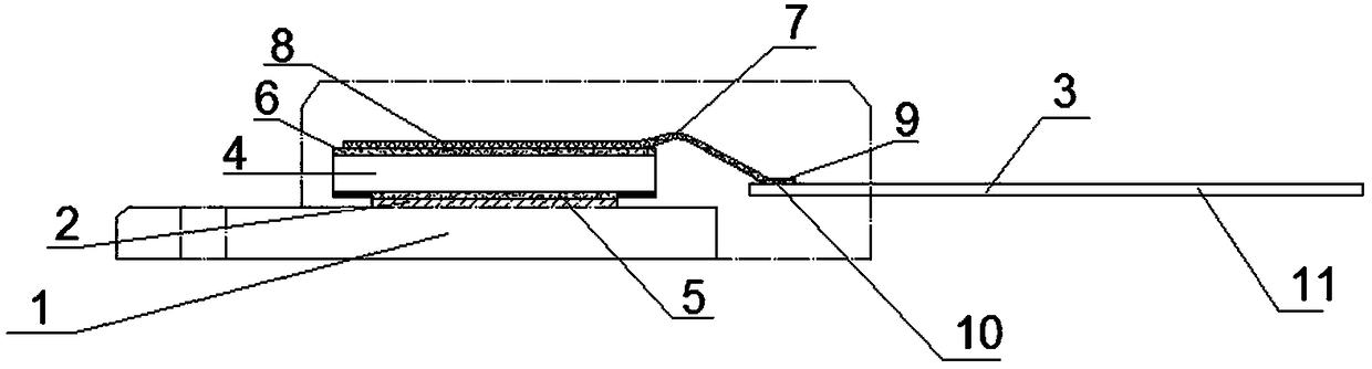
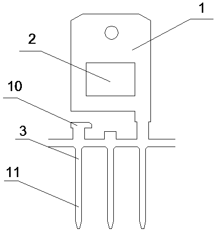
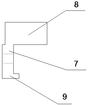
[0023] Such as Figure 1-6 As shown, a plastic-encapsulated SiC Schottky diode device includes a metal heat dissipation base plate 1, outer pins 3, a SiC Schottky diode chip 4, and a connecting bridge piece 7. A boss 2 is provided in the center area of ​​the top of the metal heat dissipation base plate 1. The outer pin 3 includes an outer pin welding area 10 and an outer pin lead-out 11, the SiC Schottky diode chip 4 includes a downward-facing anode region 5 and an upward-facing cathode region 6, and the connecting bridge 7 includes a connecting bridge Weld the A area 8, connect the bridge piece and weld the B area 9, the anode area 5 of the SiC Schottky diode chip 4 facing downward is welded on the top of the boss 2 by solder, and the cathode area 6 of the SiC Schottky diode chip 4 facing upward The soldering material is connected to the connecting bridge piece welding area A 8, and the connecting bridge piece welding area B 9 is connected to the outer pin welding area 10 thr...


PUM


Abstract

The invention discloses a plastic-encapsulated SiC Schottky diode device, which comprises a metal cooling bottom plate, an outer pin, a SiC Schottky diode chip and a connection bridge plate. The manufacturing method comprises steps: the metal cooling bottom plate is placed in a die, and an appropriate solder paste is applied to the upper surface of a boss of the metal cooling bottom plate; the anode surface of the SiC Schottky diode chip is placed on the upper surface of the boss in a downward and upside down mode, and an appropriate solder paste is applied to the upward cathode area surface of the SiC Schottky diode chip and the soldering area of the outer pin at the same time; a soldering A area and a soldering B area of the connection bridge plate are placed on the cathode area and thesoldering area of the outer pin respectively; and the product which is well assembled and the die are together subjected to one time vacuum sintering, after sintering is completed, cleaning and plastic encapsulation are carried out, encapsulation is completed and a product is formed. The chip cooling effects are greatly improved, the process is shortened, the production efficiency is improved, thedevice circulation ability is greatly improved, and the high circulation ability advantage of the SiC Schottky diode chip is thoroughly executed.

Description

technical field [0001] The invention relates to the field of power semiconductor devices, in particular to a plastic-encapsulated SiC Schottky diode device and a manufacturing method thereof. Background technique [0002] At present, the plastic-encapsulated SiC Schottky diodes on the market are all welded on the heat dissipation base plate in the cathode area, and the anode area is connected to the external pin through the aluminum wire bonding process. Compared with silicon Schottky diode chips, SiC Schottky diode chips have many advantages, such as high critical breakdown field strength and high thermal conductivity. SiC Schottky diode chips can pass larger currents and have more Excellent thermal conductivity. However, due to the low fusing current value of the aluminum wire and poor surge resistance, and the limitation of the size of the plastic-encapsulated device, the number of aluminum wire bonding is limited, which limits the flow capacity of the plastic-encapsulat...

Claims


Application Information

Patent Timeline
Patent Type & Authority Applications(China)
IPC IPC(8): H01L29/872H01L23/367H01L21/329
CPCH01L23/367H01L29/66143H01L29/872H01L2224/32245H01L2224/48247H01L2224/73265H01L2924/181H01L2924/00012H01L2924/00
Inventor 钱清友王成森徐洋范敏波江林华
Owner 捷捷半导体有限公司
Why Eureka
Try Eureka