Preparation method of cathode isolation column of organic light emitting display

A technology of light-emitting display devices and isolation columns, which is applied in the manufacture of semiconductor/solid-state devices, electric solid-state devices, semiconductor devices, etc., can solve problems affecting the life of light-emitting devices, diffusion, evaporation, and water vapor residues, etc., to improve OLED devices. Effects of longevity, pixel resolution improvement, and fewer steps

CN108539054AActive Publication Date: 2018-09-14SUZHOU WEIYEDA TOUCH TECH +2
6 Cites 9 Cited by

Patent Information

Authority / Receiving Office
CN · China
Patent Type
Applications(China)
Current Assignee / Owner
Publication Date
2018-09-14

Smart Images

  • Figure 1
    Figure 1
  • Figure 2
    Figure 2
  • Figure 3
    Figure 3
Patent Text Reader

Abstract

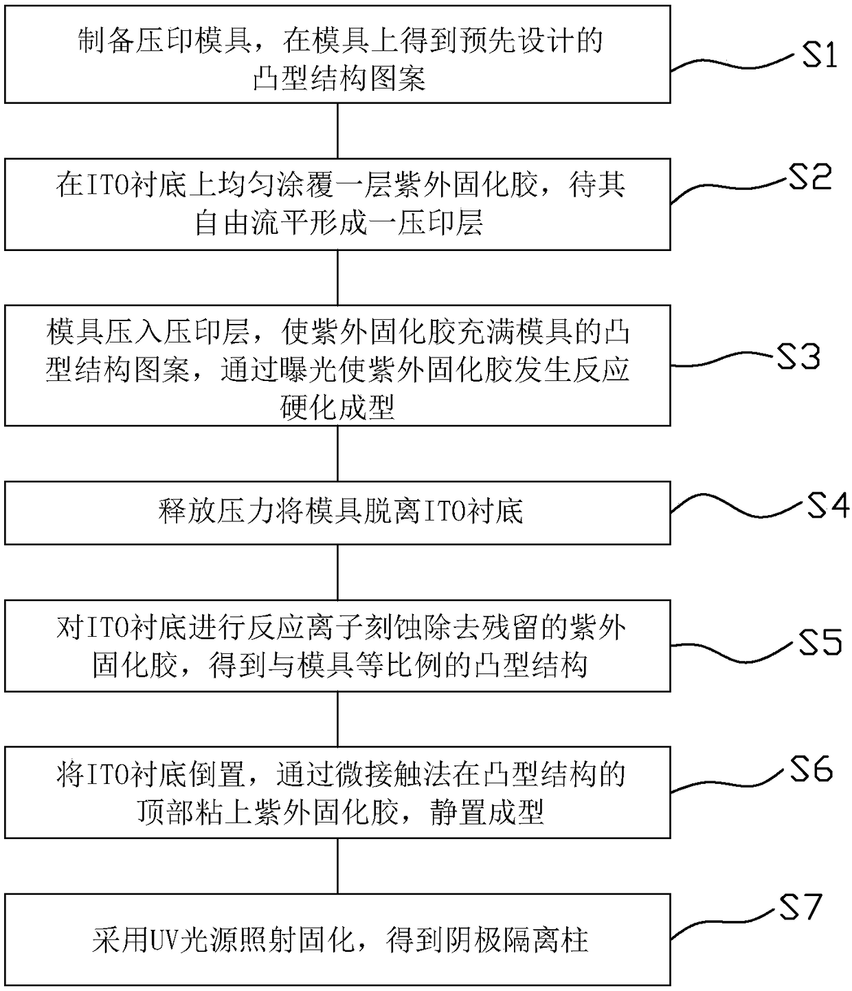
The invention discloses a preparation method of a cathode isolation column of an organic light emitting display (OLED). The preparation method comprises the following steps: firstly, preparing a coining mold, and obtaining a predesigned convex structural pattern on the mold; uniformly applying a layer of ultraviolet solidification glue on an ITO substrate, and allowing the ultraviolet solidification glue to freely flow to be flat and form a coining layer; pressing the mold in the coining layer, filling the convex structural pattern of the mold with the ultraviolet solidification glue, and through exposure, enabling the ultraviolet solidification glue to have a reaction to be hardened and formed; releasing pressure to separate the mold from the ITO substrate; performing reactive ion etchingon the ITO substrate to remove remained ultraviolet solidification glue, and obtaining a convex structure of which the ratio is the same as that of the mold; inverting the ITO substrate, adhering theultraviolet solidification glue to the top of the convex structure through a micro contact method, and performing standing forming; and performing irradiation solidification with an UV light source,so as to obtain the cathode isolation column. According to the preparation method disclosed by the invention, an ultraviolet coining technology is adopted, so that the cathode isolation column is prepared under room temperature and constant pressure; the preparation method is simple in technology and few in steps, and besides, moisture cannot be introduced; the device life of the OLED is greatly prolonged; and the pixel resolution is obviously increased.
Need to check novelty before this filing date? Find Prior Art

Description

technical field

[0001] The invention relates to a technology for a cathode isolation column of an organic light-emitting display device, in particular to a preparation method for a cathode isolation column of an organic light-emitting display device. Background technique

[0002] OLED (Organic Light Emitting Display), an organic light-emitting display device, has attracted extensive attention and in-depth research due to its characteristics of high brightness, wide viewing angle, flexibility and light weight. An organic light-emitting device generally consists of a first electrode (transparent anode), a luminescent medium deposited on the first electrode, and a second electrode (cathode) deposited on the luminescent medium. In order to achieve high resolution and colorization of passive matrix OLEDs, and better solve the problems of low cathode template resolution and low device yield, people have introduced stripe structures with inverted trapezoidal or T-shaped cross-secti...

Examples

Embodiment Construction

[0027] In order to further explain the technical means and effects of the present invention to achieve the intended purpose of the invention, the specific implementation, structure, features and effects of the present invention will be described in detail below in conjunction with the accompanying drawings and examples.

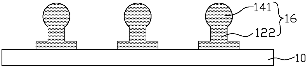
[0028] The invention provides a method for preparing a cathode isolation column of an organic light-emitting display device. see Figures 1 to 3f Shown, described preparation method comprises the steps:

[0029] S1) if Figure 3a As shown, an imprinting mold 11 is prepared, and a pre-designed convex structure pattern is obtained on the mold 11 . Specifically, in this step, the imprinting mold 11 is prepared by electron beam lithography using transparent quartz that can allow ultraviolet rays to pass through. In other embodiments, the imprinting mold 11 can also be prepared by plasma etching, laser holographic interference and other technical methods.

[0...