

Non-volatile ferroelectric random access memory and preparation process thereof
A random access memory, non-volatile technology, applied in the direction of electric solid-state devices, circuits, electrical components, etc., can solve the problems of uneven thermal budget of ferroelectric capacitors, reduce the uniformity and stability of film performance, and complicated processes, etc., to achieve The effect of high storage density, low manufacturing cost, and simple process
- Summary
- Abstract
- Description
- Claims
- Application Information
AI Technical Summary
Problems solved by technology
Method used
Image

Examples
Embodiment 1
[0045] The invention proposes a nonvolatile ferroelectric random access memory and a preparation process.
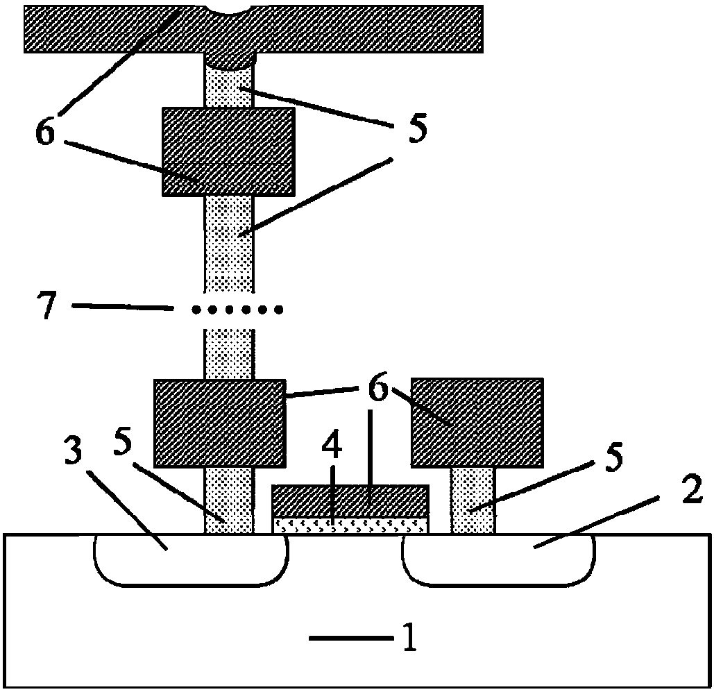
[0046] refer to figure 2 , complete the source region (2), drain region (3), gate dielectric layer (4), through holes (5), necessary metal electrodes (6) and metal wiring (7) of the transistor.
[0047]Among them, the p-type silicon substrate is the substrate, the source / drain region is n-type silicon, and the gate dielectric layer is HfO 2 The insulating film has a thickness of 5 nm. The design of the transistor is compatible with the current 0.13μm process node, and the three-layer metal wiring is completed, and the metal used is Cu.
[0048] The current 0.13μm node process can also adopt the through-hole design of the double-layer damascene structure.
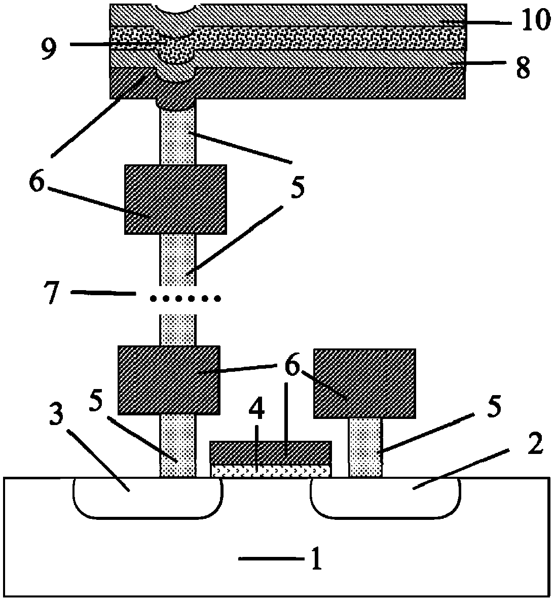
[0049] The integration process of the hafnium oxide-based ferroelectric capacitor provided by the present invention mainly refers to Figure 3-5 . It includes a bottom electrode (8), a hafnium oxide-based ferroel...
PUM
| Property | Measurement | Unit |
|---|---|---|
| Surface roughness | aaaaa | aaaaa |
| Thickness | aaaaa | aaaaa |
| Thickness | aaaaa | aaaaa |
Abstract
Description
Claims
Application Information