
Semiconductor structures and methods of forming them

A technology of semiconductor and dummy gate, which is applied in the field of semiconductor structure and its formation, can solve the problems of reducing the critical size of SRAM and the difficulty of manufacturing SRAM, and achieves the effect of good performance

Active Publication Date: 2020-07-10
SEMICON MFG INT (SHANGHAI) CORP +1
View PDF5 Cites 0 Cited by
  • Summary
  • Abstract
  • Description
  • Claims
  • Application Information

AI Technical Summary

Problems solved by technology

[0004] However, the reduced critical size of the SRAM makes the manufacture of the SRAM more difficult

Method used


Image

  • Semiconductor structures and methods of forming them
  • Semiconductor structures and methods of forming them
  • Semiconductor structures and methods of forming them

Examples


Embodiment Construction

[0034] As mentioned in the background art, the manufacturing of SRAM in the prior art is relatively difficult.

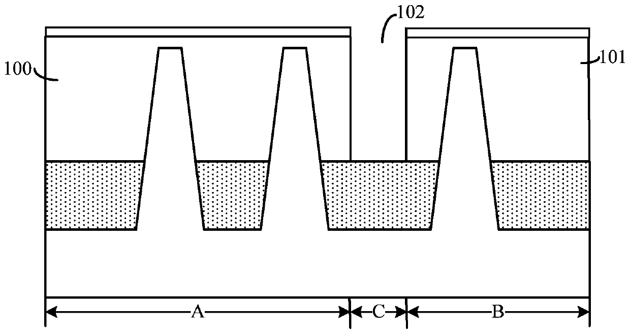
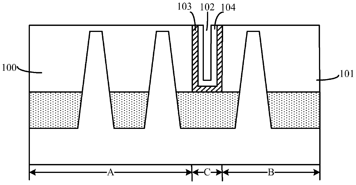
[0035] Figure 1 to Figure 2 It is a schematic diagram of each step of a method for forming a semiconductor structure.

[0036] Please refer to figure 1 , Provide a substrate, the substrate includes: a first area A, a second area B and a third area C, the third area C is located between the first area A and the second area B; in the first area A first dummy gate structure 100 is formed on the substrate of the region A, a second dummy gate structure 101 is formed on the substrate of the second region B; a dielectric opening 102 is formed on the substrate of the third region C, and the dielectric opening 102 exposes the substrate of the third region C.

[0037] The first area A is used to form a pull-up transistor, the second area B is used to form an output transistor, and the third area C is used to form the gate structure of the pull-up transistor and the output transist...


PUM

PropertyMeasurementUnit
thicknessaaaaaaaaaa
thicknessaaaaaaaaaa
thicknessaaaaaaaaaa

Abstract

A semiconductor structure and a method for forming the same, wherein the method includes: providing a substrate, the substrate including a first region, a second region and a third region, the third region being located between the first region and the second region; forming a dummy gate structure extending from the first region to the second region, the dummy gate structure passing through the third region; forming first source and drain doped regions in the substrate on both sides of the dummy gate structure in the first region respectively ; Forming second source-drain doped regions in the substrate on both sides of the dummy gate structure in the second region; after forming the first source-drain doped region and the second source-drain doped region, forming through the dummy A dielectric opening of the gate structure, the dielectric opening exposes the base of the third region; an interlayer dielectric layer is formed in the dielectric opening, and the top surface of the interlayer dielectric layer is flush with the top surface of the dummy gate structure . The method can reduce the difficulty of forming an interlayer dielectric layer in the dielectric opening.

Description

Technical field [0001] The present invention relates to the technical field of semiconductor manufacturing, in particular to a semiconductor structure and a method of forming the same. Background technique [0002] With the improvement of the integration of semiconductor devices, the key size of static random access memory (SRAM) is continuously reduced. [0003] The SRAM cell in the prior art usually has a 6T structure. A common SRAM cell with 6T structure usually includes a storage unit and two read-write units. The memory cell includes two pull-up transistors and two pull-down transistors. The two pull-up transistors are connected to the word line, and the two pull-down transistors are connected to the ground line. The memory cell has two storage nodes and two open nodes for storage. 1 or 0 signal; two read-write units are two transfer transistors, one end of each transfer transistor is connected to a storage node and an open node of the memory cell, and the other end is conne...

Claims


Application Information

Patent Timeline
Patent Type & Authority Patents(China)
IPC IPC(8): H01L21/8244H01L21/28H01L21/762H01L27/11H01L29/423H10B10/00
CPCH01L21/28008H01L21/76224H01L29/42356H10B10/12H01L27/092H01L21/823878H01L21/823864H01L21/823828H01L29/66545H01L21/823821H01L21/845H01L21/02271H01L21/823814H01L29/6656H01L21/0217H01L21/02164H01L29/6653H01L21/32115H01L27/0924H01L29/0847
Inventor 周飞
Owner SEMICON MFG INT (SHANGHAI) CORP
Learn More