Novel power module of packaging structure

A power module and packaging structure technology, applied in electrical components, electrical solid devices, circuits, etc., can solve problems such as voltage overshoot, burned modules, system interference, etc., to reduce voltage overshoot, increase mutual inductance, reduce The effect of package inductance

Pending Publication Date: 2018-09-28
NORTH CHINA ELECTRIC POWER UNIV (BAODING)
View PDF10 Cites 2 Cited by
  • Summary
  • Abstract
  • Description
  • Claims
  • Application Information

AI Technical Summary

Problems solved by technology

Due to the fast switching speed of silicon carbide MOSFETs, large voltage overshoots will be generated across them during switching transients and short-circuit conditions, which will interfere with the system. When these spikes exceed the rated voltage and current values ​​of silicon carbide MOSFETs It will degrade the performance of the power module, and even burn the module in severe cases

Method used


Image

  • Novel power module of packaging structure
  • Novel power module of packaging structure
  • Novel power module of packaging structure

Examples


Embodiment Construction

[0024] The following will clearly and completely describe the technical solutions in the embodiments of the present invention with reference to the accompanying drawings in the embodiments of the present invention. Obviously, the described embodiments are only some, not all, embodiments of the present invention. Based on the embodiments of the present invention, all other embodiments obtained by persons of ordinary skill in the art without making creative efforts belong to the protection scope of the present invention.

[0025] The above objects, features and advantages can be more clearly understood, and the present invention will be further described in detail below in conjunction with the accompanying drawings and specific embodiments.

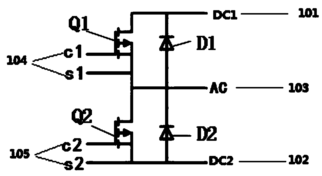
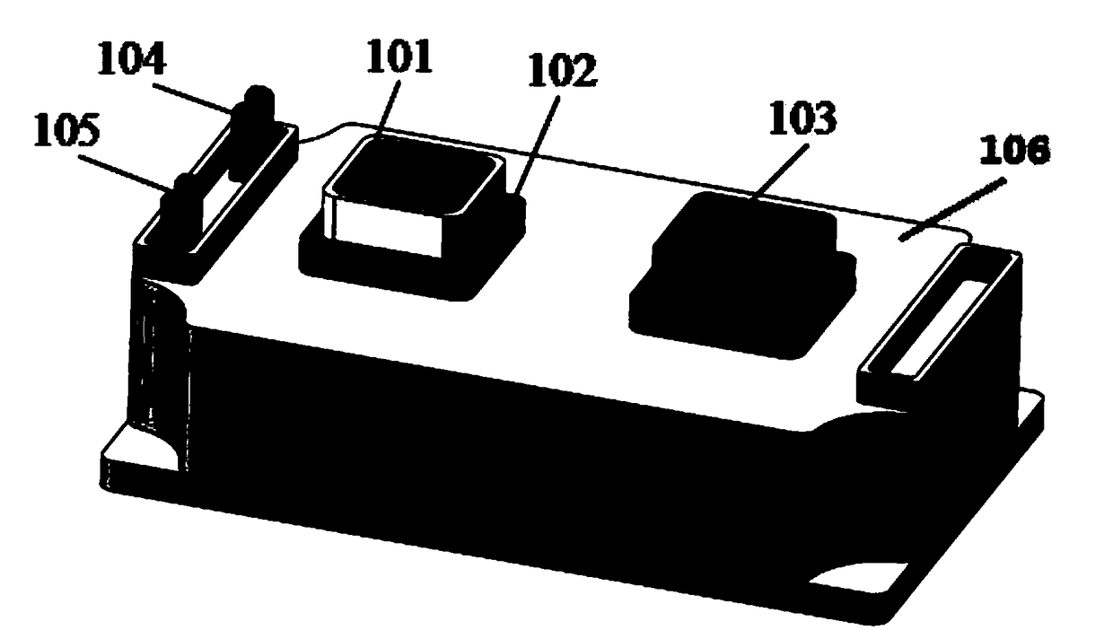
[0026] figure 1 It is a structural diagram of a power module with a new packaging structure provided by an embodiment of the present invention. Such as figure 1 As shown, a power module with a new package structure includes: a first DC si...


PUM


Abstract

The invention discloses a novel power module of a packaging structure. The power module comprises a first direct-current side terminal, a second direct-current side terminal, an alternating-current side terminal, a first drive terminal, a second drive terminal, a first silicon carbide metallic oxide semiconductor field-effect tube, a second silicon carbide metallic oxide semiconductor field-effecttube, a diode and a base, wherein the first direct-current side terminal, the second direct-current side terminal, the alternating-current side terminal, the first drive terminal and the second driveterminal are arranged on the upper surface of the base; and the first direct-current side terminal and the second direct-current side terminal are positioned on the same axis. According to the direct-current side terminals of coaxial structures provided by the invention, the distance between the direct-current side terminals can be reduced effectively, the coupling area is increased, the mutual inductance of the direct-current side terminals is increased, the packaging inductance of the power module is reduced, the voltage overshoot of the silicon carbide MOSFETs inside the power module in switching transient and short-circuited conditions is further reduced, and the switching loss of the power module is reduced.

Description

technical field [0001] The invention relates to the field of packaging of power semiconductor modules, in particular to a power module with a new packaging structure. Background technique [0002] At present, the performance of traditional silicon-based devices has reached the limit of its materials, and its application range cannot be further expanded. Therefore, a new generation of power semiconductor devices has been developed. Among these new semiconductor devices, silicon carbide power devices are widely used in high temperature, high voltage, high frequency and other fields due to their superior material properties such as wide bandgap, high critical electric field breakdown strength, high thermal conductivity, and high electron mobility. a wide range of applications. [0003] Silicon carbide metal-oxide-semiconductor field-effect transistor (Metal-Oxide-Semiconductor Field-Effect Transistor, MOSFET) device has fast switching speed, low switching loss, and small on-re...

Claims


Application Information

Patent Timeline
Patent Type & Authority Applications(China)
IPC IPC(8): H01L25/18H01L23/49
CPCH01L25/18H01L23/49
Inventor 谢宗奎邹琦柯俊吉徐鹏赵志斌崔翔
Owner NORTH CHINA ELECTRIC POWER UNIV (BAODING)
Why Eureka
Try Eureka