Eureka AIR delivers breakthrough ideas for toughest innovation challenges, trusted by R&D personnel around the world.

MEMS device, preparation method thereof and electronic device

A technology of electronic devices and devices, which is applied in the field of MEMS devices and its preparation, can solve problems such as easy fracture of the diaphragm edge and sacrifice of microphone performance

Inactive Publication Date: 2018-10-02
SEMICON MFG INT (SHANGHAI) CORP +1
View PDF17 Cites 3 Cited by
  • Summary
  • Abstract
  • Description
  • Claims
  • Application Information

AI Technical Summary

Problems solved by technology

[0005] When the microphone is working, if the sound is relatively loud, because the diaphragm is relatively thin and needs to vibrate, the edge of the diaphragm is easy to break first
If the thickness of the diaphragm is simply increased, the performance of the microphone will be sacrificed, which is unacceptable

Method used


Image

  • MEMS device, preparation method thereof and electronic device
  • MEMS device, preparation method thereof and electronic device
  • MEMS device, preparation method thereof and electronic device

Examples


preparation example Construction

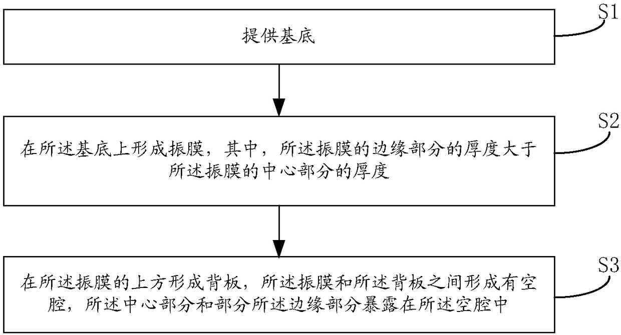
[0068] The present invention also provides a method for preparing a MEMS device, the method comprising:

[0069] providing a base 201;

[0070] forming a diaphragm on the substrate, wherein an edge portion of the diaphragm is thicker than a central portion of the diaphragm;

[0071] A back plate 206 is formed above the diaphragm, a cavity is formed between the diaphragm and the back plate, and the central portion and part of the edge portion are exposed in the cavity.

[0072] Wherein, the method for forming the diaphragm includes:

[0073] forming a diaphragm body above the base;

[0074] An auxiliary diaphragm is formed, and the auxiliary diaphragm is stacked with the edge portion of the diaphragm body and fixed together.

[0075] Specifically, the method for forming the auxiliary diaphragm includes:

[0076] forming and patterning an auxiliary diaphragm material on the substrate to remove the auxiliary diaphragm material located in a central region of the diaphragm, the...

Embodiment 1

[0085] The MEMS devices include:

[0086] Base 201;

[0087] a diaphragm located above the base, the thickness of the edge portion of the diaphragm is greater than the thickness of the central portion of the diaphragm;

[0088] a back plate 206, located above the diaphragm;

[0089] A cavity is located between the diaphragm and the back plate, the central part and part of the edge part are exposed in the cavity.

[0090] Wherein, the diaphragm includes:

[0091] The diaphragm body 204 is located above the base;

[0092] The auxiliary diaphragm 203 is stacked with the edge portion of the diaphragm body and fixed together.

[0093] Optionally, the upper and lower positions of the diaphragm body and the auxiliary diaphragm can be set arbitrarily, for example, the diaphragm body is located above the auxiliary diaphragm, or the auxiliary diaphragm is located at the top of the diaphragm body. Above all can realize the purpose of the present invention.

[0094] Such as Figure...

Embodiment 2

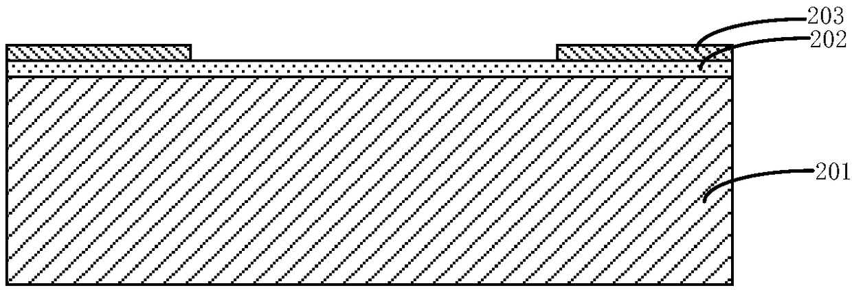
[0110] In order to solve the problems in the prior art, the present invention provides a method for manufacturing MEMS devices, which will be further described below in conjunction with the accompanying drawings. in, Figures 2a-2j It is a schematic diagram of the preparation process of the MEMS device described in the present invention; image 3 is an external view of an example of a mobile phone handset in the present invention.

[0111] figure 1 The process flow chart for the preparation of the MEMS device described in the present invention specifically includes the following steps:

[0112] Step S1: providing a substrate;

[0113] Step S2: forming a diaphragm on the base, wherein the thickness of the edge portion of the diaphragm is greater than the thickness of the central portion of the diaphragm;

[0114] Step S3: forming a back plate above the diaphragm, a cavity is formed between the diaphragm and the back plate, and the central part and part of the edge parts are...


PUM


Abstract

The invention relates to a MEMS device, a preparation method thereof and an electronic device. The MEMS device comprises a substrate, a vibration diaphragm positioned above the substrate, a backplatepositioned above the vibration diaphragm and a cavity positioned between the vibration diaphragm and the backplate, thickness of the edge portion of the vibration diaphragm is greater than that of thecentral portion of the same, and the central portion and part of the edge portion are exposed in the cavity. The vibration diaphragm thickened at a vibration edge can make thickness of the vibrationdiaphragm at a weak point to reach two or more times of that of a vibration middle area, so that sound tolerant strength is improved, falling resistance and maximum sound threshold value of the deviceare improved, and reliability of the device is improved greatly.

Description

technical field [0001] The invention relates to the field of semiconductors, in particular, the invention relates to a MEMS device, a preparation method thereof, and an electronic device. Background technique [0002] With the continuous development of semiconductor technology, in the market of sensor (motion sensor) products, smart phones, integrated CMOS and micro-electromechanical system (MEMS) devices have increasingly become the most mainstream and advanced technology, and with the update of technology, The development direction of this kind of transmission sensor products is smaller size, high-quality electrical performance and lower loss. [0003] Among them, MEMS sensors are widely used in automotive electronics: such as TPMS, engine oil pressure sensor, air pressure sensor of automobile brake system, automobile engine intake manifold pressure sensor (TMAP), common rail pressure sensor of diesel engine; consumer electronics: such as tire pressure gauge , sphygmomano...

Claims


Application Information

Patent Timeline
IPC IPC(8): B81B3/00B81C1/00
Inventor 王贤超
Owner SEMICON MFG INT (SHANGHAI) CORP
Why Eureka
Eureka Blog
Learn More