Three-dimensional storage structure

A technology of three-dimensional storage and storage unit, applied in the direction of electrical components, electrical solid devices, circuits, etc., can solve the problems of wafer cracking, affecting the deposition and etching process, and large bending stress of the wafer, so as to achieve the effect of ensuring the yield rate

Inactive Publication Date: 2018-10-16
WUHAN XINXIN SEMICON MFG CO LTD
View PDF4 Cites 7 Cited by
  • Summary
  • Abstract
  • Description
  • Claims
  • Application Information

AI Technical Summary

Problems solved by technology

[0003] However, because the existing technology generally stacks multiple layers on the wafer to form a stacked three-dimensional storage structure, it is easy to form stress concentration in the wafer, resulting in a large bending stress of the wafer, which affects the subsequent Deposition and etching process, which may lead to wafer cracking in severe cases
In the lithography process, the large bending stress of the wafer will also have an adverse effect on the lithography effect

Method used


Image

  • Three-dimensional storage structure

Examples


Embodiment Construction

[0023] The present invention will be further described below in conjunction with the accompanying drawings and embodiments.

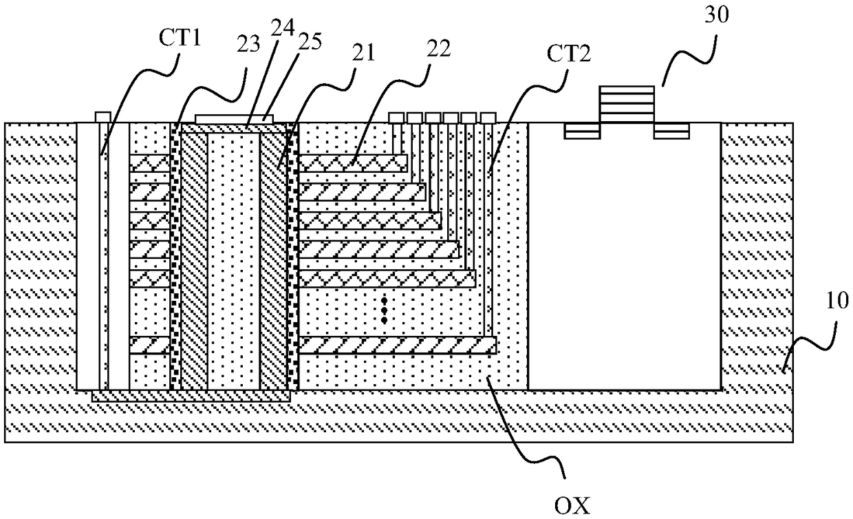
[0024] In a preferred embodiment, as figure 1 As shown, a three-dimensional memory structure is proposed, which may include a substrate 10; a plurality of grooves in an array are formed on the substrate 10; a memory cell structure is formed in each groove:

[0025] Each memory cell structure can include:

[0026] An annular and vertical columnar channel layer 21 for connecting a source and a drain;

[0027] a plurality of control gate layers 22 spaced from each other up and down, and each control gate layer 22 surrounds the columnar channel layer 21;

[0028] An annular and vertical columnar isolation layer 23, used to isolate the columnar channel layer 21 from each control gate layer 22;

[0029] Wherein, each memory cell structure is formed with a first contact hole CT1 for connecting the columnar channel layer 21 , and each second contact hole CT2...


PUM


Abstract

The invention relates to the technical field of semiconductors, in particular to a three-dimensional storage structure. The three-dimensional storage structure comprises a substrate, wherein a plurality of grooves are formed in the substrate in an array way, a storage unit structure is formed in each groove, each storage unit structure comprises an annular and vertical columnar channel layer, a plurality of control gate layers and an annular and vertical columnar isolation layer, the annular and vertical columnar channel layer is used for connecting a source and a drain, the plurality of control gate layers are vertically separated, the columnar channel layer is encircled by each control gate layer, the annular and vertical columnar isolation layer is used for separating the columnar channel layer from each control gate layer, a first contact hole and a second contact hole are formed in each storage unit structure, the first contact hole is used for connecting the columnar channel layer, and the second contact hole is used for connecting each control gate layer. By the three-dimensional storage structure, stress contraction can be prevented from being formed in a wafer of the storage structure, and the yield of a wafer product is favorably ensured.

Description

technical field [0001] The invention relates to the technical field of semiconductors, in particular to a three-dimensional storage structure. Background technique [0002] With the development of semiconductor technology, three-dimensional storage technology has been able to realize the three-dimensional storage unit, which saves more space, lower cost and higher storage capacity than traditional storage technology. [0003] However, because the existing technology generally stacks multiple layers on the wafer to form a stacked three-dimensional storage structure, it is easy to form stress concentration in the wafer, resulting in a large bending stress of the wafer, which affects the subsequent The deposition and etching process may lead to wafer cracking in severe cases. In the photolithography process, the large bending stress of the wafer will also have an adverse effect on the photolithography effect. Contents of the invention [0004] In view of the above problems,...

Claims


Application Information

Patent Timeline
Patent Type & Authority Applications(China)
IPC IPC(8): H01L27/11556H01L27/11521H01L27/11568H01L27/11582H01L27/11526H01L27/11573
CPCH10B41/30H10B41/40H10B41/27H10B43/30H10B43/40H10B43/27
Inventor 谢岩丁振宇刘选军
Owner WUHAN XINXIN SEMICON MFG CO LTD
Why Eureka
Try Eureka