On-chip infrared LED based on two-dimensional material heterojunction and its preparation method

A two-dimensional material and heterojunction technology, which is applied in the field of on-chip infrared LED and preparation based on two-dimensional material heterojunction, can solve the problems of low luminous efficiency, on-chip light source, and inability to integrate, so as to improve radiation efficiency and enhance The effect of restriction

Active Publication Date: 2020-04-21
INST OF SEMICONDUCTORS - CHINESE ACAD OF SCI +1
View PDF2 Cites 0 Cited by
  • Summary
  • Abstract
  • Description
  • Claims
  • Application Information

AI Technical Summary

Problems solved by technology

However, there is a very serious defect in silicon-based optical interconnection so far, that is, the problem of on-chip light source, because silicon is an indirect bandgap semiconductor, and its luminous efficiency is extremely low, so it cannot be integrated.
Therefore, it is often necessary to use gratings to introduce external light sources, but this method will inevitably increase the complexity of the process and the difficulty of packaging

Method used


Image

  • On-chip infrared LED based on two-dimensional material heterojunction and its preparation method
  • On-chip infrared LED based on two-dimensional material heterojunction and its preparation method
  • On-chip infrared LED based on two-dimensional material heterojunction and its preparation method

Examples


preparation example Construction

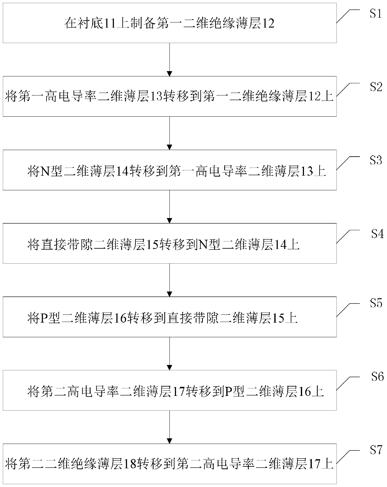
[0054] In the second exemplary embodiment of the present disclosure, a method for manufacturing an on-chip infrared LED based on a two-dimensional material heterojunction is provided, image 3 It is a flow chart of a method for an on-chip infrared LED based on a novel two-dimensional material according to an embodiment of the present disclosure. Such as image 3 As shown, the present disclosure provides a method for preparing an LED on a chip using a novel two-dimensional material, including the following steps:

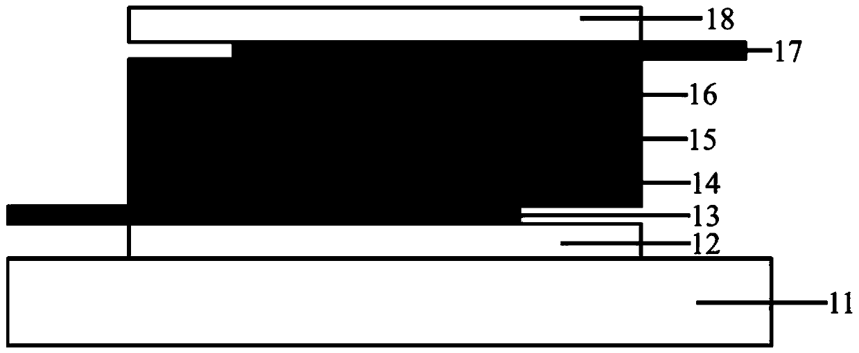
[0055] Step S1: preparing a first two-dimensional insulating thin layer 12 on the substrate 11;

[0056] Step S2: the first two-dimensional thin layer with high conductivity 13 is transferred onto the first two-dimensional insulating thin layer 12 by a transfer method;

[0057] Step S3: transferring the N-type two-dimensional thin layer 14 onto the first high-conductivity two-dimensional thin layer 13;

[0058] Step S4: transferring the direct bandgap two-dimensio...


PUM

PropertyMeasurementUnit
transmittivityaaaaaaaaaa

Abstract

The disclosure provides an on-chip infrared LED based on a two-dimensional material heterojunction. The on-chip infrared LED is composed of a substrate, a first thin two-dimensional insulating layer,a first thin high-conductivity two-dimensional layer, a thin N type two-dimensional layer, a thin direct band gap two-dimensional layer, a thin P type two-dimensional layer, a thin second high-conductivity two-dimensional layer, and a thin second two-dimensional insulating layer that are arranged successively from bottom to top. According to the disclosure, no lattice mismatch problem is caused; the light-emitting wavelength can be adjusted to a certain extent by changing the thickness of a thin layer of an active region and integration with a silicon-based photonic device is realized; the restriction on the active region carriers is enhanced and the radiation efficiency is improved; and a light source problem of silicon-based on-chip light interconnection is solved, so that the on-chip optical communication is realized.

Description

technical field [0001] The present disclosure relates to the field of manufacturing light-emitting diodes in the field of optoelectronics, in particular to an on-chip infrared LED based on a two-dimensional material heterojunction and a preparation method thereof. Background technique [0002] The discovery of graphene not only brought surprises to theoretical physicists, but what is even more exciting is that it has unique and excellent physical properties in mechanics, electricity, optics and other aspects. It is the thinnest and hardest nanomaterial found so far. Its band gap is zero, but its transmittance to light exceeds 97%, and its electron mobility exceeds 15000 cm at room temperature. 2 V -1 the s -1 , making graphene have great application prospects in the fields of high-frequency electronic devices and transparent electrodes. On the other hand, the zero bandgap of graphene also limits its application in the fields of electronics and optoelectronics, so a large ...

Claims


Application Information

Patent Timeline
Patent Type & Authority Patents(China)
IPC IPC(8): H01L33/02H01L33/18H01L33/26H01L33/00
CPCH01L33/005H01L33/02H01L33/18H01L33/26
Inventor 刘思捷魏钟鸣李京波
Owner INST OF SEMICONDUCTORS - CHINESE ACAD OF SCI
Why Eureka
Try Eureka