Method for growing gallium oxide epitaxial layer by adopting halide vapor phase epitaxy method

A technology of vapor phase epitaxy and epitaxial growth, which is applied in the direction of electrical components, semiconductor/solid-state device manufacturing, circuits, etc., and can solve the problems of less epitaxial layer reporting and insufficient depth of epitaxial growth, etc.

Inactive Publication Date: 2021-09-14
CHINA ELECTRONICS TECH GRP NO 46 RES INST
View PDF5 Cites 0 Cited by
  • Summary
  • Abstract
  • Description
  • Claims
  • Application Information

AI Technical Summary

Problems solved by technology

However, the current domestic 2 o 3 The research on epitaxial growth is not deep enough, Ga 2 o 3 The epitaxial layer is rarely reported

Method used


Image

  • Method for growing gallium oxide epitaxial layer by adopting halide vapor phase epitaxy method
  • Method for growing gallium oxide epitaxial layer by adopting halide vapor phase epitaxy method
  • Method for growing gallium oxide epitaxial layer by adopting halide vapor phase epitaxy method

Examples


Embodiment 1

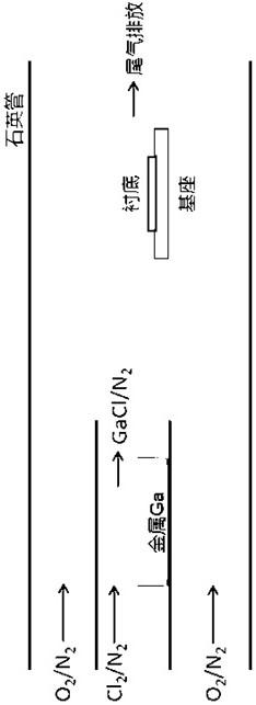
[0025] A method for growing a gallium oxide epitaxial film by halide vapor phase epitaxy, the steps comprising:

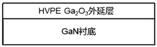
[0026] (1) Growth of α-Ga on a GaN single wafer as a substrate 2 o 3 epitaxial layer. Before the start of epitaxial growth, the substrate was heated successively with acetone and absolute ethanol in a water bath at 90°C for 20 minutes, and then ultrasonically cleaned with ultrapure water for 10 minutes to remove organic and inorganic impurities on the surface.

[0027] (2) Place the substrate sheet in (1) under a differential interference microscope to observe its appearance, and confirm that the surface of the substrate sheet is clean and smooth, free of paraffin wax, attached particles, scratches, and damage.

[0028] (3) Put the substrate sheet in (2) horizontally on the base, and send it to the growth temperature zone of the halide vapor phase epitaxy tube furnace.

[0029] (4) Close the horizontal tube furnace, extract the vacuum for 20 minutes, and repeate...

Embodiment 2

[0035] A method for growing a gallium oxide epitaxial film by halide vapor phase epitaxy, the steps comprising:

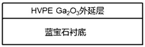
[0036] (1) Growth of β-Ga on sapphire substrate 2 o 3 epitaxial layer. Before the start of epitaxial growth, the substrate was heated successively with acetone and absolute ethanol in a water bath at 90°C for 20 minutes, and then ultrasonically cleaned with ultrapure water for 10 minutes to remove organic and inorganic impurities on the surface.

[0037] (2) Place the substrate sheet in (1) under a differential interference microscope to observe its appearance, and confirm that the surface of the substrate sheet is clean and smooth, free of paraffin wax, attached particles, scratches, and damage.

[0038] (3) Put the substrate sheet in (2) horizontally on the base, and send it to the growth temperature zone of the halide vapor phase epitaxy tube furnace.

[0039] (4) Close the horizontal tube furnace, extract the vacuum for 20 minutes, and repeatedly flush the c...

Embodiment 3

[0045] A method for growing a gallium oxide epitaxial film by halide vapor phase epitaxy, the steps comprising:

[0046] (1) With β-Ga 2 o 3 Homogeneous growth of β-Ga on single crystal as substrate 2 o 3 epitaxial layer. Before the start of epitaxial growth, the substrate was heated successively with acetone and absolute ethanol in a water bath at 90°C for 20 minutes, and then ultrasonically cleaned with ultrapure water for 10 minutes to remove organic and inorganic impurities on the surface.

[0047] (2) Place the substrate sheet in (1) under a differential interference microscope to observe its appearance, and confirm that the surface of the substrate sheet is clean and smooth, free of paraffin wax, attached particles, scratches, and damage.

[0048] (3) Put the substrate sheet in (2) horizontally on the base, and send it to the growth temperature zone of the halide vapor phase epitaxy tube furnace.

[0049] (4) Close the horizontal tube furnace, extract the vacuum for...


PUM


Abstract

The invention provides a method for growing a gallium oxide epitaxial layer by adopting a halide vapor phase epitaxy method, which comprises the following steps: taking three wafers, namely sapphire, GaN and [beta]-Ga2O3 single crystal, as a substrate, epitaxially growing a Ga2O3 epitaxial layer by adopting the halide vapor phase epitaxy method, and controlling the temperature and the growth pressure of a growth region and regulating and controlling the VI/III ratio, achieving the preparation of the epitaxial layers of the two crystal forms of [alpha]-Ga2O3 and [beta]-Ga2O3. The growth speed of the epitaxial layer obtained through the method reaches 5-10 [mu] m/h, and the XRD half-peak width of the homogeneous epitaxial layer is smaller than or equal to 100 arcsec. By adopting the scheme provided by the invention, the preparation of the thick epitaxial layer at a relatively high growth speed can be realized, the epitaxial growth research of a Ga2O3 material is effectively promoted, and a new thought is provided for subsequent Ga2O3-based device manufacturing and performance improvement.

Description

technical field [0001] The invention belongs to the field of semiconductor film material preparation, and relates to a method for growing a gallium oxide epitaxial layer by a halide vapor phase epitaxy method, that is, epitaxial deposition of gallium oxide is realized on different substrates by the halide vapor phase epitaxy method. Background technique [0002] Gallium oxide (Ga 2 o 3 ) material, as a new type of wide-bandgap semiconductor material, has high withstand voltage and low loss characteristics, as well as good chemical and thermal stability, and has broad applications in high-power devices, solar-blind ultraviolet detection, gas sensors, etc. The prospect has attracted more and more domestic and foreign researchers' attention. But Ga 2 o 3 Materials research is still in its infancy, especially Ga 2 o 3 Epitaxial film quality is not high. At present, several commonly used preparations of Ga 2 o 3 Epitaxial film methods include: molecular beam epitaxy (MBE...

Claims


Application Information

Patent Timeline
Patent Type & Authority Applications(China)
IPC IPC(8): H01L21/02
CPCH01L21/02472H01L21/0262
Inventor 李贺赖占平董增印程文涛张嵩
Owner CHINA ELECTRONICS TECH GRP NO 46 RES INST
Why Eureka
Try Eureka