A kind of porous gan conductive dbr and preparation method thereof

A porosity and electrochemical technology, applied in circuits, electrical components, semiconductor devices, etc., can solve the problems of low repetition rate, harsh conditions, poor conductivity of AlGaN materials, and achieve simple preparation methods, adjustable center wavelength, high The effect of reflectivity

Active Publication Date: 2020-10-30
SHANDONG UNIV
View PDF3 Cites 0 Cited by
  • Summary
  • Abstract
  • Description
  • Claims
  • Application Information

AI Technical Summary

Problems solved by technology

[0003] For the nitride DBR of AlN / GaN system, the stress caused by the lattice mismatch of the AlGaN / GaN DBR structure will cause the DBR to crack. At the same time, the AlGaN material has poor conductivity, which affects the photoelectric performance of the device.
Although in AlInN / GaN DBR, AlInN and GaN can be lattice-matched by adjusting the ratio of Al and In, because the growth rate of AlInN is slow, and the refractive index of AlGaN, AlInN and GaN is relatively close, it often requires dozens of pairs of 1 / 4λ thickness AlGaN / GaN requires a long growth time, so the DBR growth procedure is complicated, the conditions are harsh and the repetition rate is not high
[0004] The GaN / Air structure DBR prepared by etching the conductive GaN layer by conductivity-selective electrochemical etching technology has a maximum reflectivity of more than 50%, but the structure of the GaN / Air structure DBR is unstable and non-conductive

Method used


Image

  • A kind of porous gan conductive dbr and preparation method thereof
  • A kind of porous gan conductive dbr and preparation method thereof
  • A kind of porous gan conductive dbr and preparation method thereof

Examples


Embodiment 1

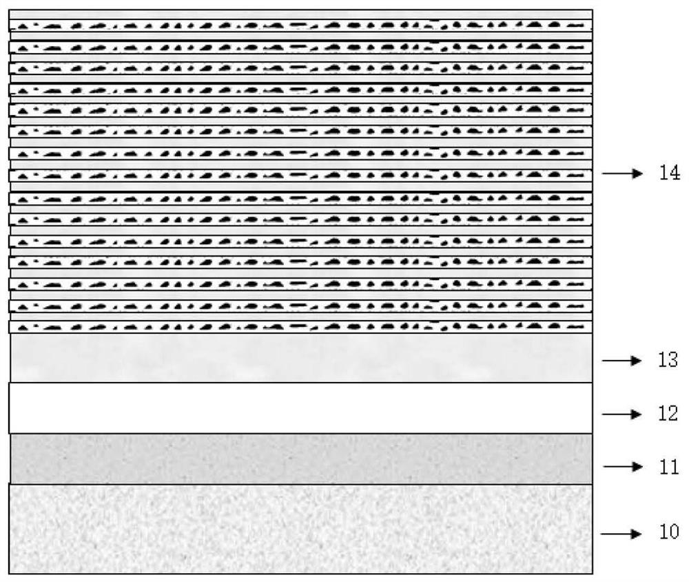
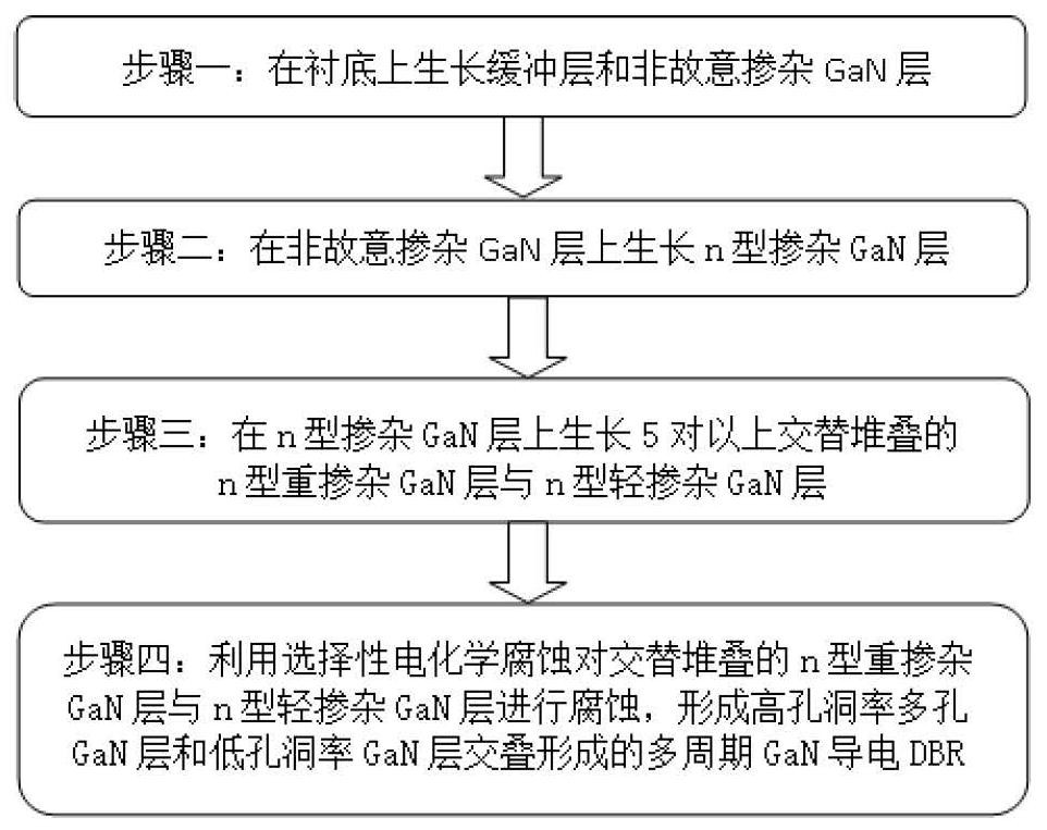
[0042] A porous GaN conductive DBR, such as figure 1 As shown, it includes a substrate 10, a buffer layer 11, an unintentionally doped GaN layer 12, an n-type intentionally doped gallium nitride layer 13 and a porous GaN conductive DBR layer 14 grown sequentially from bottom to top;

[0043]The porous GaN conductive DBR layer 14 is formed by alternately stacking 15 pairs of high-porosity porous GaN layers and low-porosity porous GaN layers, the porosity of the high-porosity porous GaN layer is 52%, and the porosity of the low-porosity porous GaN layer is 0 (i.e. no holes).

Embodiment 2

[0045] A porous GaN conductive DBR, the structure is as shown in embodiment 1, the difference is that the dopant of the n-type doped GaN layer 13 is silicon, and the doping concentration is 3×10 18 cm -3 .

Embodiment 3

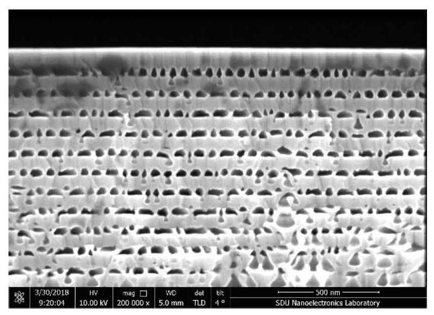
[0047] A porous GaN conductive DBR, the structure is as shown in Example 1, the difference is that the high-porosity porous GaN layer and the low-porosity porous GaN layer are alternately stacked n-type heavily doped GaN by electrochemical corrosion respectively. Layer and n-type lightly doped GaN layer are etched, the dopant of n-type lightly doped GaN layer and n-type heavily doped GaN layer is silicon, the higher the doping concentration, the higher the porosity formed, as image 3 As shown, it is a cross-sectional scanning electron microscope schematic diagram of a porous GaN conductive DBR structure at a magnification of 200,000 times. The holes formed by the n-type heavily doped GaN layer after electrochemical corrosion are relatively uniform, and the pore diameter is between 1 and 300 nm; while The uncorroded GaN layer is an n-type lightly doped GaN layer, and the two layers of materials have a refractive index difference due to the introduction of air holes, and are alt...


PUM

PropertyMeasurementUnit
pore sizeaaaaaaaaaa
reflectanceaaaaaaaaaa

Abstract

The invention relates to a porous GaN conductive DBR and a preparation method thereof. The porous GaN conductive DBR comprises a substrate, a buffer layer, an unintentionally doped GaN layer, an n-type intentionally doped gallium nitride layer and a porous GaN conductive DBR layer which are sequentially grown from bottom to top, wherein the porous GaN conductive DBR layer is formed by alternatelystacking high-hole-rate porous GaN layers and low-hole-rate porous GaN layers. The porous GaN conductive DBR does not have the lattice mismatch problem, is simple in structure, and has the characteristics of high reflectivity, good conductivity and adjustable central wavelength.

Description

technical field [0001] The invention relates to a porous GaN conductive DBR and a preparation method thereof, belonging to the field of photoelectric technology. Background technique [0002] Group-III nitride wide bandgap semiconductor materials are widely used in optoelectronics and electric power such as lighting, display and medical treatment due to their unique physical characteristics such as large bandgap width, coverage from infrared to ultraviolet, strong breakdown field, high temperature resistance, acid and alkali resistance, etc. It is widely used in the field of electronics. With the continuous deepening of research on gallium nitride materials and devices, gallium nitride optoelectronic devices will surely be applied to more optoelectronic fields, such as high-end lighting, optical communication, laser display, etc. Therefore, it is of great scientific significance and application value to develop a simple and low-cost technology by in-depth study of the struc...

Claims


Application Information

Patent Timeline
Patent Type & Authority Patents(China)
IPC IPC(8): H01L33/10H01L33/46H01S5/183
CPCH01L33/10H01L33/46H01S5/18366
Inventor 张宇魏斌
Owner SHANDONG UNIV
Why Eureka
Try Eureka