Method of manufacturing of a solar cell and solar cell thus obtained

A technology for solar cells, tunnel dielectrics, used in final product manufacturing, sustainable manufacturing/processing, semiconductor/solid-state device manufacturing, etc.

Inactive Publication Date: 2018-10-23
TEMPRESS IP
View PDF9 Cites 12 Cited by
  • Summary
  • Abstract
  • Description
  • Claims
  • Application Information

AI Technical Summary

Problems solved by technology

Thus, it appears that the nitride barrier slows down boron migration through the tunnel dielectric, but does not completely prevent it

Method used


Image

  • Method of manufacturing of a solar cell and solar cell thus obtained
  • Method of manufacturing of a solar cell and solar cell thus obtained
  • Method of manufacturing of a solar cell and solar cell thus obtained

Examples


Embodiment Construction

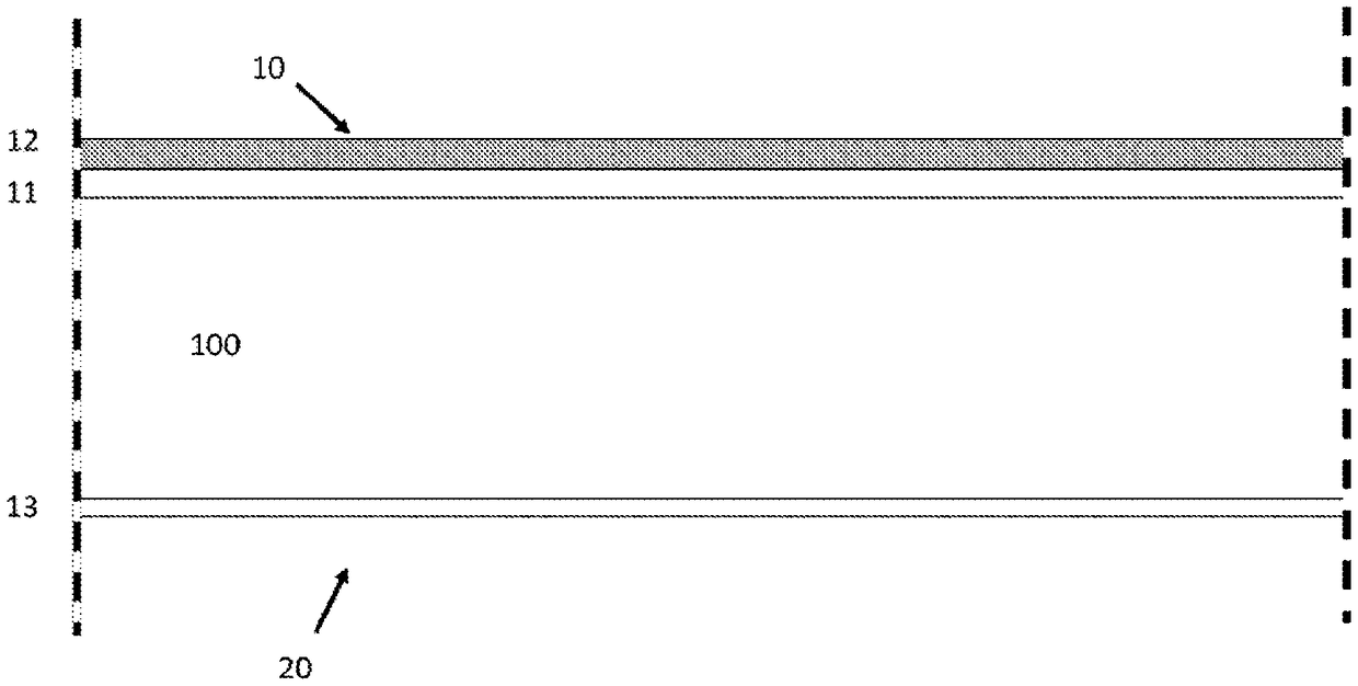
[0091] utensils such as Figure 1C and Figure 1D The test structure for the configuration shown in Complete Preliminary Results. A monocrystalline silicon substrate is used which is doped n-type in a manner conventional to the skilled person. More than one substrate is provided into the reaction chamber of the LPCVD apparatus. The substrate is then processed according to the invention. A tunnel dielectric with a thickness of 1.5 nm was applied by thermal oxidation. Thereafter, a multilayer stack of silicon layers and boron dopant layers is applied. The multilayer stack starts and ends with silicon layers. The total number of boron dopant layers is nine. The total thickness of the multilayer stack is about 400 nm, which is evenly distributed over the 10 polysilicon layers. The boron dopant layer is relatively thin. No protection is applied so that the multilayer stack grows in the same way on both sides of the silicon substrate. This is followed by annealing.

[0092...


PUM

PropertyMeasurementUnit
thicknessaaaaaaaaaa
thicknessaaaaaaaaaa
thicknessaaaaaaaaaa

Abstract

The method of manufacturing of a solar cell comprises the steps of: providing a semiconductor substrate (100) comprising an electrically conductive region (11) extending at a first side thereof; and providing a tunnelling oxide (13) by thermal oxidation followed by a boron doped polysilicon LPCVD deposited layer on the second side of the semiconductor substrate. Herein, the provision of the dopedpolysilicon layer (20) comprises depositing a multilayer stack of first sublayers (21, 22, 23) of silicon and second sublayers (31, 32) of boron dopant in alternation, and subsequent annealing. Thereafter the solar cell is finalized with passivation layers on at least the first side and suitable metallization layers on the emitter and base regions.

Description

field of invention [0001] The present invention relates to a method of manufacturing a solar cell, said method comprising the steps of: [0002] - providing a semiconductor substrate having a first side and a second side, the first side being intended as a main side for receiving light; [0003] - depositing a tunnel dielectric on at least a second side of the semiconductor substrate; [0004] - depositing a doped silicon layer onto the second side of the substrate by means of low pressure chemical vapor deposition, said doped silicon layer being separated from the substrate by a tunnel dielectric; [0005] - Anneal the doped silicon layer [0006] - further processing of the substrate into a solar cell, ie provided with a back end; [0007] The invention also relates to the solar cell arrangement thus obtained. [0008] The invention also relates to low pressure chemical vapor deposition (LPCVD) equipment. Background of the invention [0009] The efficiency and lifetim...

Claims


Application Information

Patent Timeline
Patent Type & Authority Applications(China)
IPC IPC(8): H01L31/0224H01L31/068H01L31/18C23C16/24
CPCC23C16/24C23C16/28C23C16/56H01L21/02381H01L21/0245H01L21/02488H01L21/02507H01L21/02532H01L21/02579H01L21/0262H01L31/022425H01L31/0682H01L31/0684H01L31/1804Y02E10/546Y02E10/547Y02P70/50H01L31/182
Inventor 马泰恩·莱内斯罗纳德·科内利斯·杰拉德·纳贝尔约翰尼斯·莱茵德·马克·卢奇斯艾伯特·哈斯佩尔
Owner TEMPRESS IP
Why Eureka
Try Eureka