CMOS SOI radio frequency switching circuit

A radio frequency switch and circuit technology, applied in circuits, electronic switches, electrical components, etc., can solve the problems of limiting switch switching speed, long switching time of ShuntSwitch, easy breakdown of gate oxide layer, etc.

Active Publication Date: 2018-11-02
SANECHIPS TECH CO LTD
View PDF8 Cites 4 Cited by
  • Summary
  • Abstract
  • Description
  • Claims
  • Application Information

AI Technical Summary

Problems solved by technology

figure 1 Although this type of traditional series-parallel stack structure has the advantages of large power capacity, strong ability to suppress harmonics, and high isolation, it limits the switching speed of the switch, especially the switching speed of the Shunt Switch.
In order to increase the switching speed of the Shunt Switch, the method of the related technology is to reduc

Method used


Image

  • CMOS SOI radio frequency switching circuit
  • CMOS SOI radio frequency switching circuit
  • CMOS SOI radio frequency switching circuit

Examples


Embodiment Construction

[0031] In order to make the purpose, technical solution and advantages of the present invention more clear, the embodiments of the present invention will be described in detail below in conjunction with the accompanying drawings. It should be noted that, in the case of no conflict, the embodiments in the present application and the features in the embodiments can be combined arbitrarily with each other.

[0032] The steps shown in the flowcharts of the figures may be performed in a computer system, such as a set of computer-executable instructions. Also, although a logical order is shown in the flowcharts, in some cases the steps shown or described may be performed in an order different from that shown or described herein.

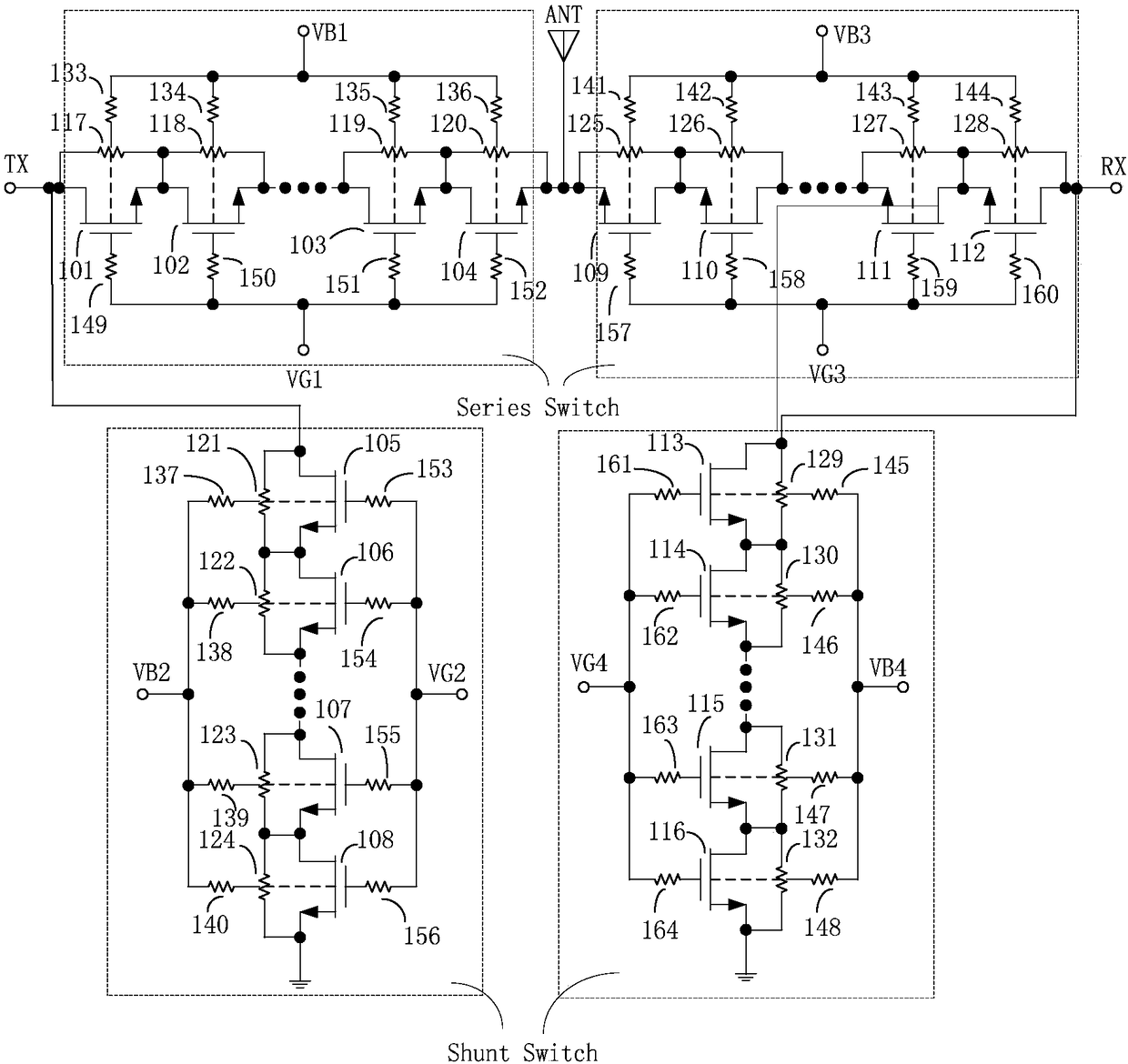
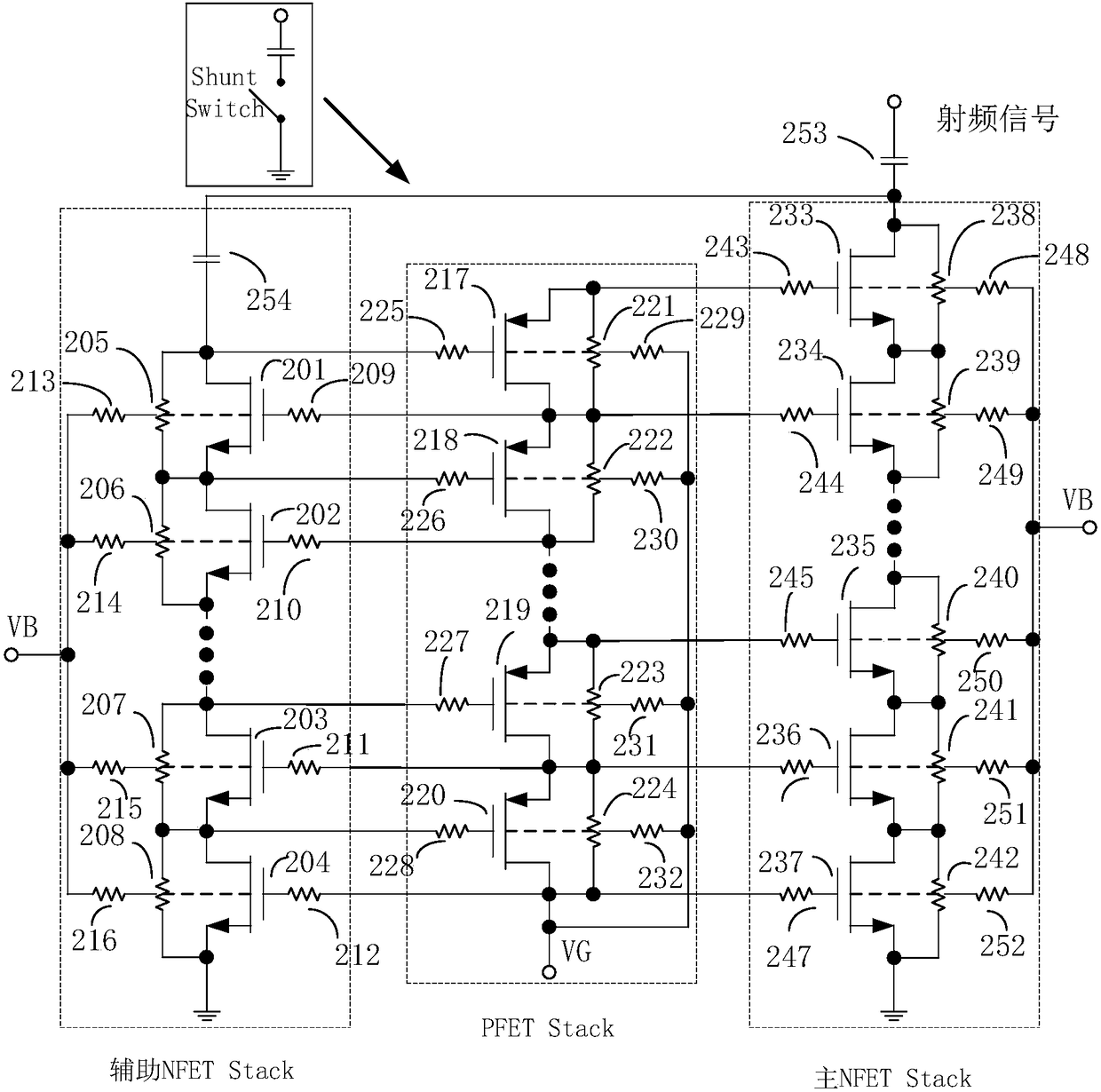
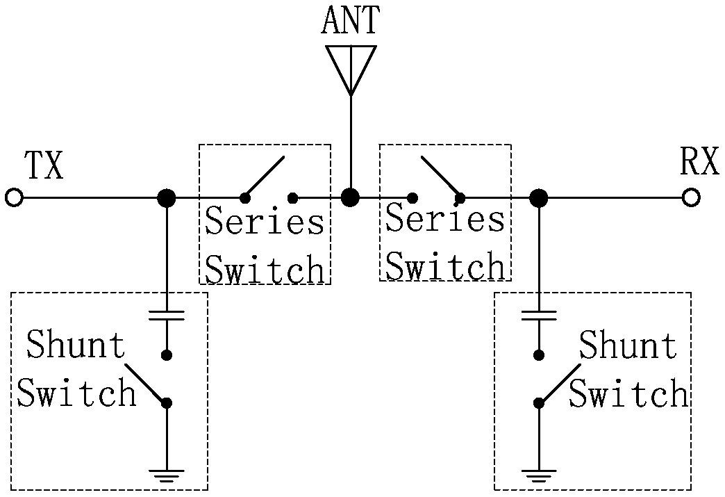
[0033] This application is in figure 1Improve and propose a CMOSSOI radio frequency switch circuit with high switching speed on the basis of the Shunt Switch in the paper. like figure 2 As shown, the CMOS SOI radio frequency switch circuit of the prese...


PUM


Abstract

The invention discloses a CMOS SOI radio frequency switching circuit. The CMOS SOI radio frequency switching circuit comprises a main NFET Stack, an auxiliary NFET Stack, a PFET Stack, a first capacitor and a second capacitor; grid electrodes of the main NFET Stack and the auxiliary NFET Stack are connected to a drain electrode and a source electrode of the PFET Stack step by step; one end of themain NFET Stack is connected to the auxiliary NFET Stack and the first capacitor, and the other end thereof is grounded; one end of the auxiliary NFET Stack is connected to the main NFET Stack and thesecond capacitor, and the other end thereof is grounded; the PFET Stack connection controls a second bias voltage; and the on-off state of the CMOS SOI radio frequency switching circuit is controlledby a first bias voltage and the second bias voltage. The CMOS SOI radio frequency switching circuit provided by the invention can increase the switching speed of a switch without reducing the grid capacitance of an NFET.

Description

technical field [0001] The invention relates to the field of radio frequency integrated circuits, in particular to a CMOS SOI radio frequency switch circuit. Background technique [0002] With the rapid development of wireless communication technology and the continuous evolution of new terminal forms, the modes and frequency bands that the RF front-end system of wireless communication mobile terminals need to support are also increasing, which undoubtedly increases the complexity of the RF front-end architecture, especially in improving system integration. At present, researchers at home and abroad are working on fully integrating the entire RF front-end system, but unfortunately, the RF transceiver (radio frequency transceiver) module and the RF PA (radio frequency power amplifier) ​​module that achieves higher output signal power are still difficult to achieve. The main reason for the on-chip integration is that the former usually adopts the traditional CMOS bulk silicon...

Claims


Application Information

Patent Timeline
IPC IPC(8): H03K17/041H03K17/687
CPCH03K17/04106H03K17/687H03K2217/0036
Inventor 朱雄辉刘斌周勇
Owner SANECHIPS TECH CO LTD
Why Eureka
Try Eureka