Supercharge Your Innovation With Domain-Expert AI Agents!

Novel seed crystal paving method during cast single crystal production

A laying method and seed crystal technology, which are applied in the directions of single crystal growth, single crystal growth, chemical instruments and methods, etc., can solve the problems of the quality decline of cast single crystals, the generation of dislocations and proliferation of seed crystals, etc., so as to improve the quality and reduce the dislocation effect

Inactive Publication Date: 2018-11-06
JIANGXI SORNID HI TECH
View PDF0 Cites 1 Cited by
  • Summary
  • Abstract
  • Description
  • Claims
  • Application Information

AI Technical Summary

Problems solved by technology

[0006] The purpose of the present invention is to provide a method for laying a new type of seed crystal in the production of cast single crystal, which solves the problem that dislocations will occur in the seed crystal in the existing method of producing cast single crystal, and these dislocations will proliferate in large quantities during subsequent crystal growth. , resulting in a serious drop in the quality of cast single crystals

Method used


Image

  • Novel seed crystal paving method during cast single crystal production
  • Novel seed crystal paving method during cast single crystal production
  • Novel seed crystal paving method during cast single crystal production

Examples


Embodiment 1

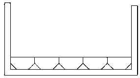
[0034] Such as figure 1 , figure 2 As shown, when producing cast single crystals, a new seed crystal and its laying method are provided, including the following steps:

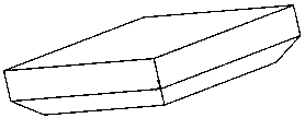
[0035] Step a: straight pull the single crystal rod to remove the edge skin, and then cut it to obtain a small cuboid-shaped seed crystal with a size of 156mm×156mm×30mm;

[0036] Step b: chamfering the four sides of the cuboid-shaped seed crystal in contact with the bottom of the crucible, the angle is 45°, and the height is 15mm;

[0037] Step c: The sides of the seed crystals are closely attached to cover the entire bottom of the crucible to form a complete seed crystal layer.

[0038] The complete seed crystal layer described in step c is formed by splicing 25 seed crystals.

Embodiment 2

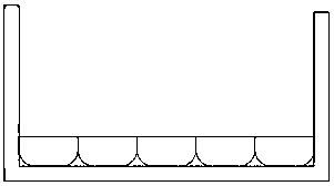
[0040] Such as image 3 , Figure 4 As shown, when producing cast single crystals, a new seed crystal and its laying method are provided, including the following steps:

[0041] Step a: straight pull the single crystal rod to remove the edge skin, and then cut it to obtain a small cuboid-shaped seed crystal with a size of 156mm×156mm×30mm;

[0042] In step b, the four sides of the cuboid-shaped seed crystal in contact with the bottom of the crucible are rounded, and the radius of the rounded corners is 15mm;

[0043] Step c: The sides of the seed crystals are closely attached to cover the entire bottom of the crucible to form a complete seed crystal layer.

[0044] The complete seed crystal layer described in step c is formed by splicing 25 seed crystals.

Embodiment 3

[0046] Such as Figure 5 , Image 6 As shown, when producing cast single crystals, a new seed crystal and its laying method are provided, including the following steps:

[0047] Step a: straight pull the single crystal rod to remove the edge skin, and then cut it to obtain a small cuboid-shaped seed crystal with a size of 156mm×156mm×30mm;

[0048] In step b, the seed crystal is further processed into a step shape, and the height of the step is 15 mm;

[0049] Step c: The sides of the seed crystals are closely attached to cover the entire bottom of the crucible to form a complete seed crystal layer.

[0050] The complete seed crystal layer described in step c is formed by splicing 25 seed crystals.

[0051] Fig. 7 is the minority carrier lifetime test diagram of cast single crystal obtained by adopting the conventional seed crystal laying method, and Fig. 8 is the minority carrier lifetime test diagram of cast single crystal obtained by adopting the new seed crystal and its...


PUM


Abstract

The invention relates to a novel seed crystal paving method during cast single crystal production. The method comprises the following steps that a single crystal rod is straightly pulled for removingedge peels; after the cutting off, seed crystals in a small cuboid shape are obtained; four edges of the seed crystals are chamfered or the seed crystals are processed into a step shape; the lateral surfaces of the seed crystals are tightly attached; the seed crystals are fully paved at the bottom of a whole crucible. At a silicon material melting stage, silicon liquid flows into seed crystal splicing seams; gaps are reserved at the bottom of the seed crystal splicing seams; the sufficient space is reserved for the silicon liquid solidification volume expansion, so that great stress cannot becaused on the seed crystals; the generation of dislocation is reduced; the quality of the cast single crystal is improved.

Description

technical field [0001] The invention relates to a method for laying a new type of seed crystal when producing cast single crystal. Background technique [0002] Crystalline silicon occupies an absolute advantage in the current solar energy material market. In terms of its crystal form, it can be divided into three categories: amorphous silicon, monocrystalline silicon, and polycrystalline silicon. The cost of amorphous silicon cells is low, but the conversion efficiency is also low, and due to the light-induced attenuation effect of amorphous silicon, its performance stability is poor; the content of impurities and defects in monocrystalline silicon cells is low, and the conversion efficiency is high, but The preparation process is complicated, and the purity of raw materials is high, so the production cost is also high; the production cost of polycrystalline silicon cells is low, but there are a large number of grain boundaries, high-density dislocations and impurities insi...

Claims


Application Information

Patent Timeline
IPC IPC(8): C30B11/14C30B29/06
CPCC30B11/14C30B29/06
Inventor 刘世龙雷琦刘超徐云飞王超姚晨张泽兴黄林赖昌权
Owner JIANGXI SORNID HI TECH
Features
  • R&D
  • Intellectual Property
  • Life Sciences
  • Materials
  • Tech Scout
  • Unparalleled Data Quality
  • Higher Quality Content
  • 60% Fewer Hallucinations
Learn More