

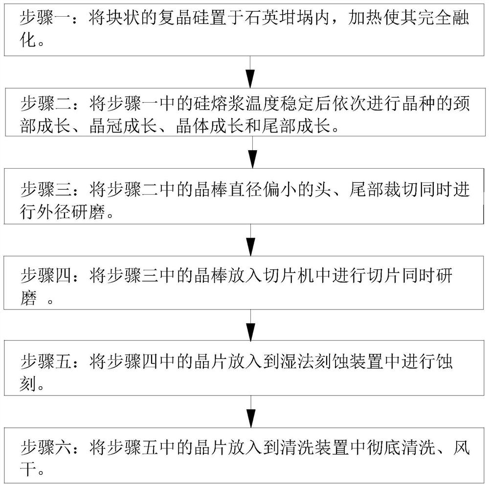
A wafer production process
A wafer and production method technology, applied in the field of wafer production technology, can solve the problems of wafer clamping, uniform etching, and technical solution limitations, etc., to increase the contact area, improve the etching effect, and increase the contact Effect
- Summary
- Abstract
- Description
- Claims
- Application Information
AI Technical Summary
Problems solved by technology
Method used
Image

Examples
Embodiment approach
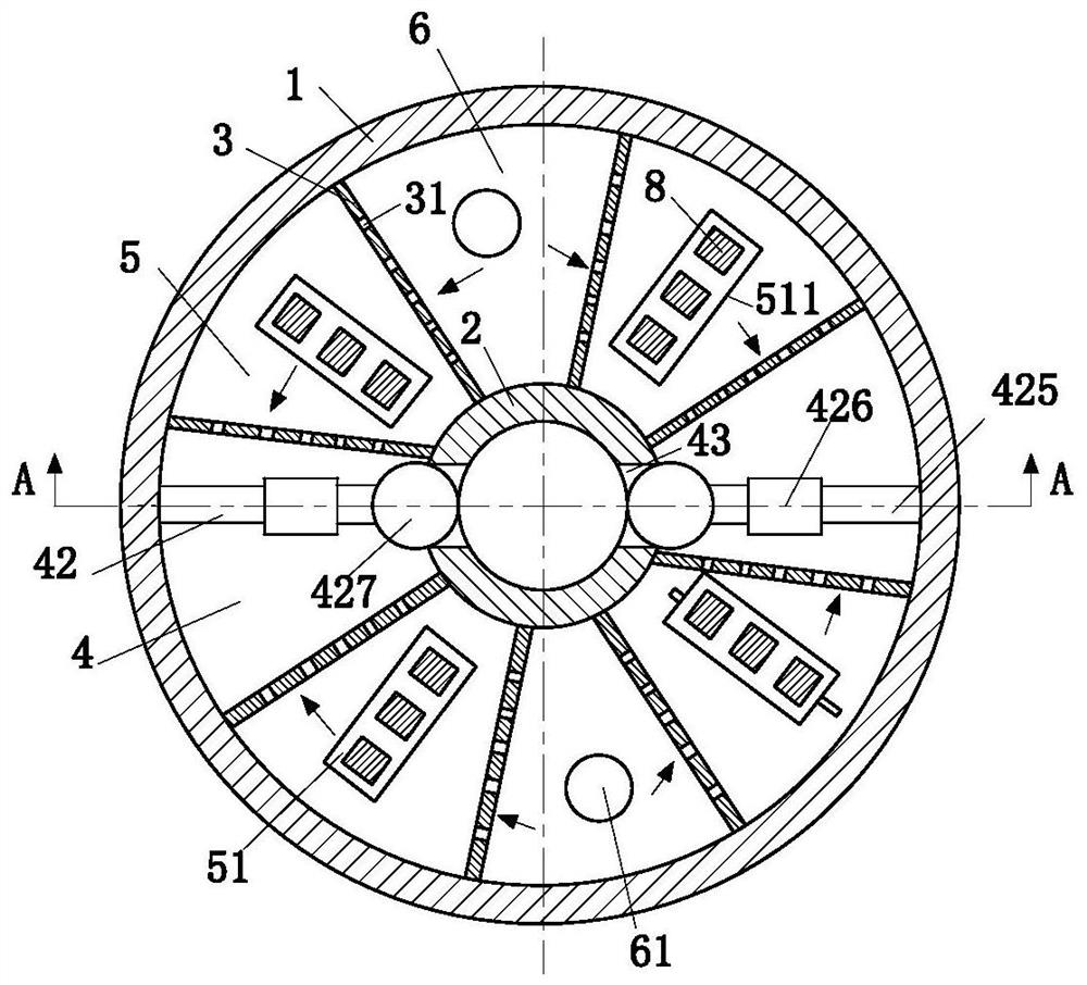
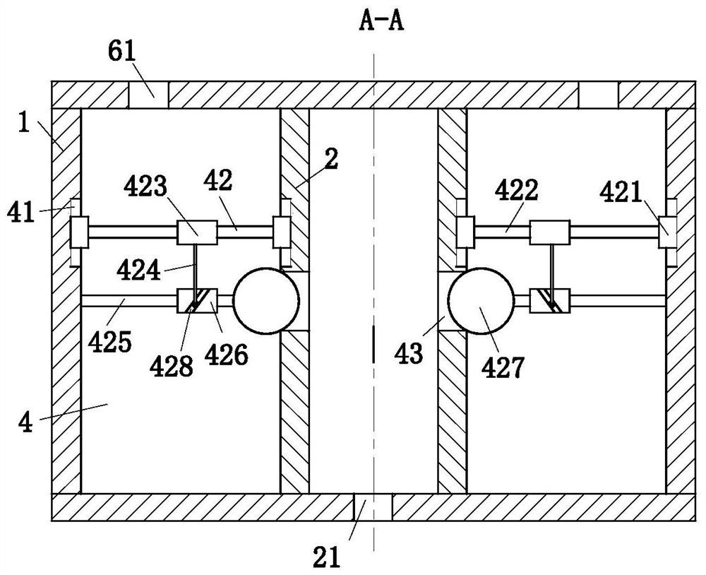
[0039] As an embodiment of the present invention, the liquid blocking module 42 includes a No. 1 slider 421, a No. 1 guide rod 422, a floating block 423, a No. 2 guide rod 424, a No. 1 sliding telescopic rod 425, and a No. 3 slider 426. and a spherical stopper 427; the floating block 423 is fixedly connected with the No. 1 slider 421 through the No. 1 guide rod 422; the No. 1 slider 421 slides on the No. 1 chute 41; the slider 423 below is provided with three No. slider 426; No. 2 chute 428 is provided in the No. 3 slider 426; One end of No. 2 guide rod 424 is connected with floating block 423; The other end of No. 2 guide rod 424 is provided with No. 2 slider 429 , which is used to drive the movement of No. 3 slider 426; said No. 3 slider 426 is fixedly connected with spherical stopper 427 through one end of No. 1 sliding telescopic rod 425, and the other end of No. 1 sliding telescopic rod 425 is connected with No. The wall is fixedly connected; the spherical stopper 427 is ...
PUM
 Abstract
Description
Claims
Application Information