An igbt device with integrated voltage sampling function

A technology for integrating voltages and devices, applied in the field of power semiconductor devices, can solve the problems of regulation, weakened electrical isolation, and reduced sampling accuracy, and achieves the effects of simple sampling structure, reduced hole accumulation, and compatible manufacturing processes

Active Publication Date: 2020-09-15
UNIV OF ELECTRONICS SCI & TECH OF CHINA
View PDF6 Cites 0 Cited by
  • Summary
  • Abstract
  • Description
  • Claims
  • Application Information

AI Technical Summary

Problems solved by technology

figure 1 It is a schematic diagram of the voltage sampling structure of a traditional IGBT device. This kind of voltage sampling structure needs to be isolated from the IGBT cell structure by "Gate Runner", which has no effect on the IGBT current conduction and requires additional chip area; at the same time As the sampling voltage level increases, the voltage value collected by the voltage sampling port will rise rapidly, the electrical isolation of the voltage sampling structure will be weakened accordingly, and the mapping relationship between the sampling voltage and the IGBT terminal voltage will also be weakened, resulting in a significant increase in sampling accuracy. decline
In addition, the traditional voltage sampling structure cannot realize the adjustment of the voltage sampling ratio when the device size is fixed, which is limited by the voltage level of the high-voltage application circuit

Method used


Image

  • An igbt device with integrated voltage sampling function
  • An igbt device with integrated voltage sampling function
  • An igbt device with integrated voltage sampling function

Examples


Embodiment Construction

[0027] The technical solution of the present invention will be described in detail and clearly below in conjunction with the accompanying drawings and specific embodiments of the description:

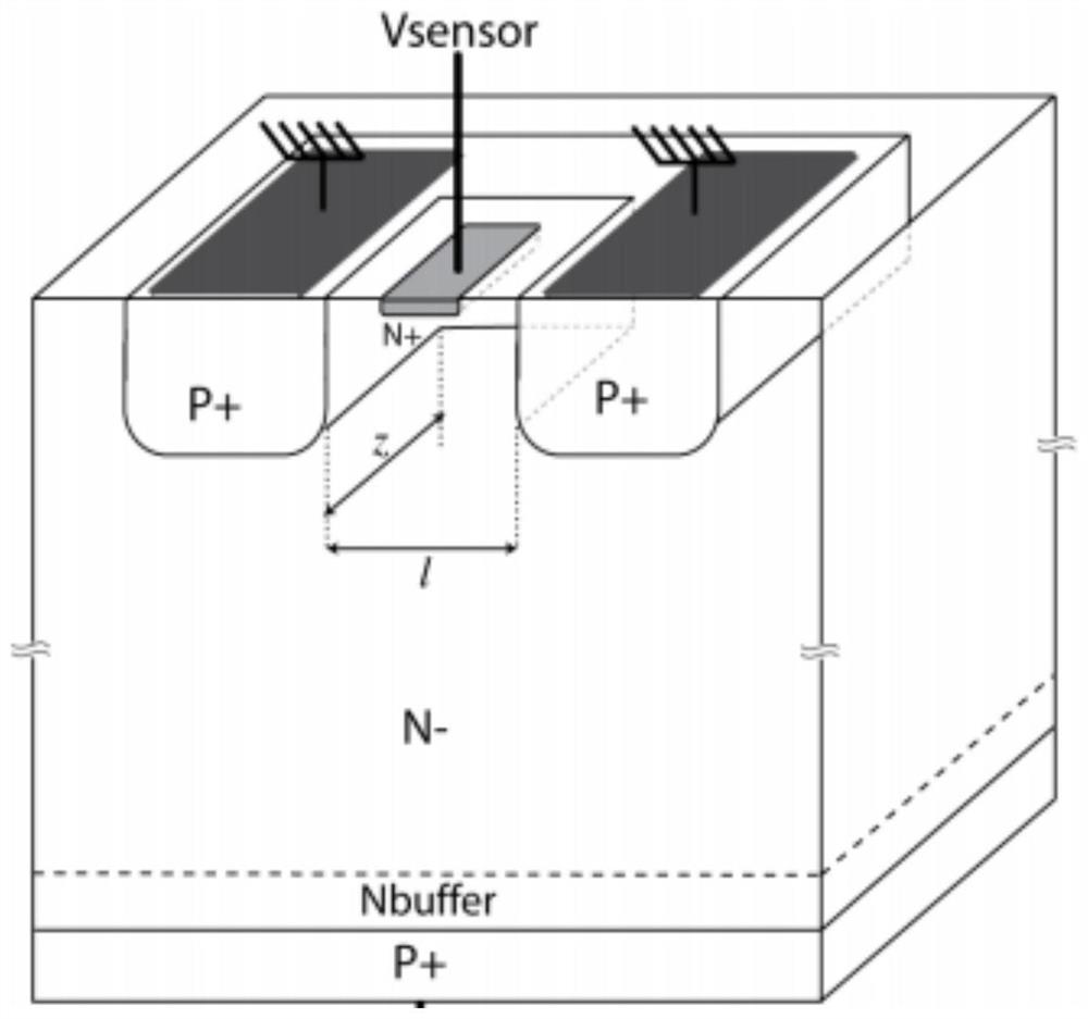
[0028] figure 1It is a schematic diagram of the voltage sampling structure of a traditional IGBT device. This kind of voltage sampling structure needs to be isolated from the IGBT cell structure by "Gate Runner", which has no effect on the IGBT current conduction and requires additional chip area; at the same time As the sampling voltage level increases, the voltage value collected by the voltage sampling port will rise rapidly, the electrical isolation of the voltage sampling structure will be weakened accordingly, and the mapping relationship between the sampling voltage and the IGBT terminal voltage will also be weakened, resulting in a significant increase in sampling accuracy. decline. In addition, the traditional voltage sampling structure cannot realize the adjustment of the vol...


PUM


Abstract

The invention provides an IGBT device with integrated voltage sampling function, which belongs to the technical field of power semiconductor devices. In the present invention, the channel of the JFET structure introduced into the body region is in a normally-off state, and in the forward conduction state of the device, the body region stores carriers, enhances conductance modulation, and reduces the saturation conduction voltage drop of the device; , the body region acts as a floating field-limiting ring, which weakens the electric field aggregation phenomenon at the bottom of the trench gate, and improves the withstand voltage reliability of the device; the gate and source of the JFET structure introduced in the present invention are respectively connected to the peripheral control circuit and the sampling port The voltage sampling function can be realized by using the mapping relationship between the source voltage change of the JFET structure and the withstand voltage of the IGBT, which will not damage the forward blocking characteristics of the device while achieving the electrical isolation effect; by changing the gate of the JFET structure The bias voltage realizes the adjustment of the voltage sampling ratio to meet the requirements of different application conditions for voltage sampling. The sampling structure of the invention is simple and compatible with the existing technology.

Description

technical field [0001] The invention belongs to the technical field of power semiconductor devices, and in particular relates to an IGBT device with an integrated voltage sampling function. Background technique [0002] With the rapid development of high-speed railways, new energy vehicles and other means of transportation, insulated gate bipolar transistors (Insulated Gate Bipolar Transistor, IGBT) have become the preferred choice in power electronics applications due to their advantages such as simple gate control, high current density, and low conduction voltage. One of the mainstream power switching devices. In order to meet the requirements of high power or ultra-high power in practical applications, IGBT devices are usually packaged in modules. In practical applications, overvoltage usually occurs at both ends of the chip, so that the blocking capability of the device is limited by avalanche breakdown, and the avalanche withstand parameter of the IGBT directly charact...

Claims


Application Information

Patent Timeline
Patent Type & Authority Patents(China)
IPC IPC(8): H01L29/739H01L29/06H01L23/544
CPCH01L22/30H01L29/0684H01L29/7397H01L29/7398
Inventor 李泽宏彭鑫贾鹏飞杨洋张金平高巍任敏张波
Owner UNIV OF ELECTRONICS SCI & TECH OF CHINA
Why Eureka
Try Eureka