Substrate integrated waveguide leaky wave slot array antenna for near-field two-dimensional scanning

A substrate-integrated waveguide and two-dimensional scanning technology, which is applied in leaky waveguide antennas, antenna arrays and antennas that are powered separately, can solve the problem of excessive unit spacing, errors, and high insertion loss characteristics that are not suitable for millimeter waves or higher frequencies. Design and other issues to achieve the effect of suppressing grating lobes and improving antenna performance

Active Publication Date: 2018-11-16
UNIV OF ELECTRONICS SCI & TECH OF CHINA
View PDF12 Cites 7 Cited by
  • Summary
  • Abstract
  • Description
  • Claims
  • Application Information

AI Technical Summary

Problems solved by technology

(4) For the frequency-swept antenna, because of the limited width, the near-field focusing phase can only be generated by the position of the antenna element, which will lead to excessive element spacing, resulting in the appearance of grating lobes and stray radiation, and the grid of the array Lobe and spurious radiation suppression methods present challenges
The first scheme is realized by combining the bent microstrip line feed network with multi-layer board technology (see: P.F.Li, S.W.Qu, S.Yang and Z.P.Nie, “Microstrip arrayantenna with 2-D steerable focus in near- field region,"IEEE Trans.AntennasPropag.,vol.65,no.9,pp.4607-4617,Sep.2017.), but the high insertion loss characteristics of traditional microstrip line and multilayer board technology are not suitable for millimeter wave or higher frequency design, and in this scheme, the antenna array synthesis method that separates the E plane and the H plane to design independently will produce large errors in the design of large array near-field focusing antennas
The second option is to modify the array width to synthesize the near-field focusing phase (see: A.J.Martínez-Ros, J.L.Gómez-Tornero, and G.Goussetis, "Holographic pattern synthesis with modulated substrate integrated waveguideline-source leaky-wave antennas," IEEE Trans.Antennas Propag.,vol.61,no.7,pp.3466–3474,Jul.2013.), but the fluctuating transmission line width will produce different responses to the frequency, resulting in the deterioration of the frequency scanning performance of the antenna, and at the same time The width of the fluctuation adds difficulty to the formation design of another dimension
The third option is to adjust the spacing of the radiating elements to achieve phase control (see: S.Clauzier, S.Avrillon, L.Le Coq, M.Himdi, F.Colombel, and E.Rochefort, "Slotted waveguide antenna with a near -fieldfocused beam in one plane,"IET Microw.Antennas Propag.,vol.9,no.7,pp.634–639,2015.), but because of the near-field square-law phase acceleration characteristics, excessive cell spacing will be generated , resulting in the appearance of grating lobes and stray radiation, which cannot meet the scanning requirements of near-field focusing

Method used


Image

  • Substrate integrated waveguide leaky wave slot array antenna for near-field two-dimensional scanning
  • Substrate integrated waveguide leaky wave slot array antenna for near-field two-dimensional scanning
  • Substrate integrated waveguide leaky wave slot array antenna for near-field two-dimensional scanning

Examples


Embodiment Construction

[0035] Below in conjunction with accompanying drawing and embodiment the present invention is described in further detail:

[0036] In this embodiment, firstly, a substrate-integrated waveguide leaky-wave slot array antenna for near-field two-dimensional scanning is provided.

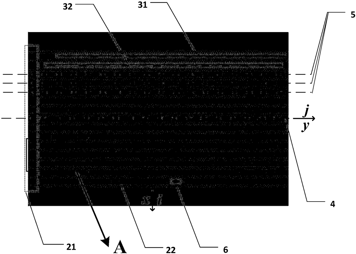
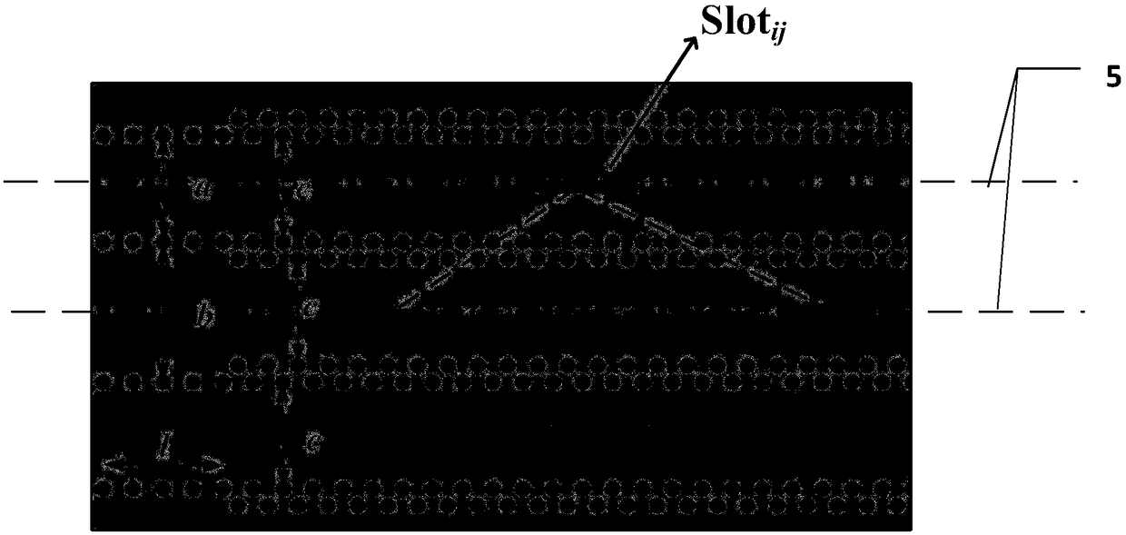
[0037] The substrate-integrated waveguide leaky-wave slot array antenna for near-field scanning is a planar structure, which includes a stacked lower metal copper clad layer 1, a dielectric substrate layer 2 and an upper metal copper clad layer 3 from bottom to top, such as figure 1 shown. Figure 2(a) shows the overall structure of the antenna. The dielectric substrate layer 2 has several rows of single-row metallized through-hole lines 21 located at the beginning of the substrate and double-row metallized through-hole lines 22 connected thereto. Each row of metallized through-hole lines includes several metallized through-hole lines. Through holes, each metallized through hole runs through the lower me...


PUM


Abstract

The invention provides a substrate integrated waveguide leaky wave slot array antenna for near-field two-dimensional scanning. A dielectric substrate layer is internally provided with a plurality of rows of single-row metalized through hole arrays and a double-row metalized through hole array which are connected with the single-row metalized through hole arrays. The distance between two adjacent rows of the single-row metalized through holes is different from that between another two adjacent rows of the single-row metalized through holes for generating a feeding phase difference. The width between two adjacent rows of the double-row metalized through holes is same with that between any other two adjacent rows of the double-row metalized through holes. An upper metal copper-plated layer isprovided with a plurality of rows of slots which vertically penetrate through the upper metal copper-plated layer, wherein the slot positions of each row of slots are different. The slots are intersected vertically and longitudinally for forming a triangular structure. In a direction from an antenna feeding end to a matching end, the distances between adjacent radiating slots gradually reduce, thereby generating phase distribution for near-field focusing. The substrate integrated waveguide leaky wave slot array antenna has advantages of realizing accurate compensation of aperture phase of a near-field two-dimensional antenna array surface, generating a design process for the near-field two-dimensional scanning substrate integrated waveguide antenna array, presenting a triangularly arranged topology, suppressing stray radiation and improving antenna performance.

Description

technical field [0001] The invention belongs to the field of near-field focusing antennas, and in particular relates to a millimeter-wave near-field two-dimensional scanning substrate integrated waveguide leaky-wave slot array antenna. Background technique [0002] With the wide application of near-field focusing antennas in the fields of microwave and millimeter wave imaging, wireless power transmission, access control and radio frequency identification, higher and higher requirements are put forward for its scanning range, scanning rate and performance. [0003] Phased array antennas can realize two-dimensional scanning to meet the scanning rate requirements of near-field applications, but they are not suitable for millimeter wave or higher frequency bands due to their complex structure and high cost. In order to realize high-frequency and high-speed near-field two-dimensional scanning, it is an effective form to combine one-dimensional frequency scanning and one-dimension...

Claims


Application Information

Patent Timeline
Patent Type & Authority Applications(China)
IPC IPC(8): H01Q1/48H01Q13/22H01Q21/06
CPCH01Q1/48H01Q13/22H01Q21/068
Inventor 程钰间吴亚飞柏航樊勇宋开军张波林先其张永鸿
Owner UNIV OF ELECTRONICS SCI & TECH OF CHINA
Why Eureka
Try Eureka