Semiconductor structure and formation method thereof

A semiconductor and transistor area technology, applied in the field of semiconductor structure and its formation, can solve the problems affecting the performance of semiconductor structure, etc., and achieve the effects of reducing leakage current, high quality, and convenient process operation

Active Publication Date: 2018-11-23
SEMICON MFG INT (SHANGHAI) CORP +1
View PDF6 Cites 0 Cited by
  • Summary
  • Abstract
  • Description
  • Claims
  • Application Information

AI Technical Summary

Problems solved by technology

[0005] However, the method of forming the semiconductor structure e

Method used


Image

  • Semiconductor structure and formation method thereof
  • Semiconductor structure and formation method thereof
  • Semiconductor structure and formation method thereof

Examples


Example Embodiment

[0032] The wafer test structure of the present invention will be described in more detail below in conjunction with schematic diagrams, wherein a preferred embodiment of the present invention is represented, it should be understood that those skilled in the art can modify the present invention described here, and still realize the beneficial effects of the present invention . Therefore, the following description should be understood as the broad knowledge of those skilled in the art, but not as a limitation of the present invention.

[0033] There are many problems in the formation method of the semiconductor structure, and it is difficult to guarantee the stable performance of the formed semiconductor structure.

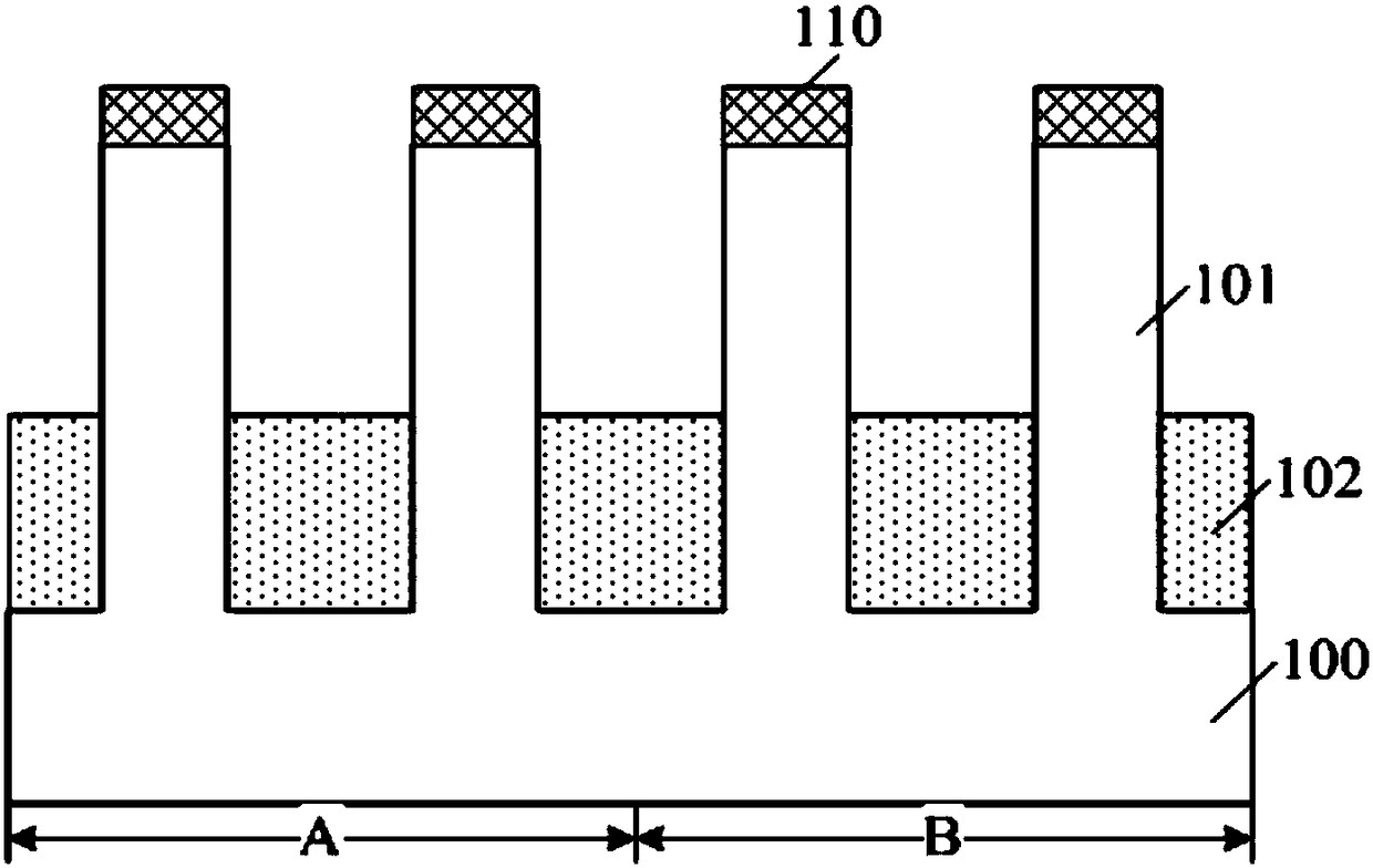
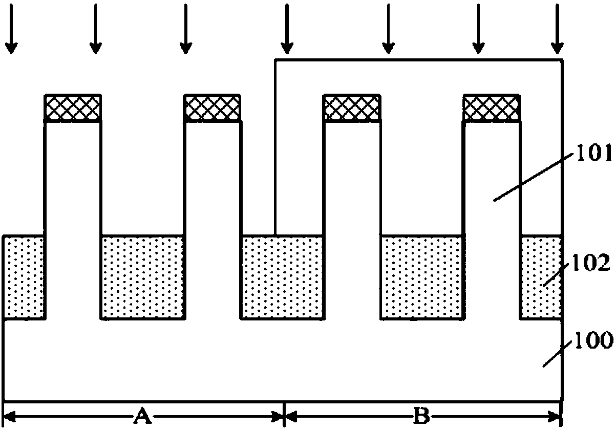
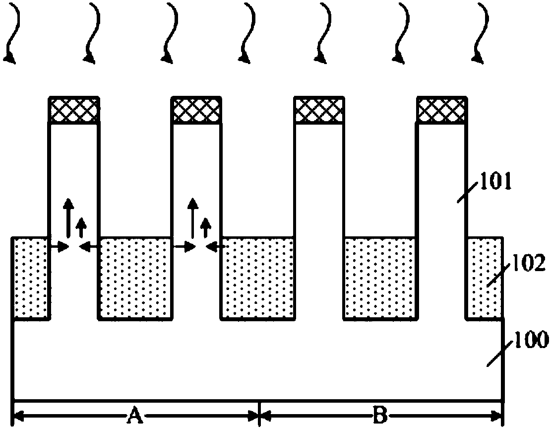
[0034] After research, it is found that as the size of the fin used to form the fin field effect transistor continues to shrink, the bottom of the source region and the drain region formed in the fin is prone to bottom punch through (punch through), that is, the sou...


PUM


Abstract

A formation method of a semiconductor structure comprises the following steps: providing a substrate, wherein fin parts are arranged on the substrate, and a fin part gap is kept between every two adjacent fin parts; arranging a hard mask above the fin parts; forming a punchthrough-proof layer above the hard mask, wherein the punchthrough-proof layer is filled with punchthrough-proof ions; formingan anti-spreading layer which is lower than the fin parts, and injecting anti-spreading ions into the fin part gaps, wherein the anti-spreading ions can prevent the punchthrough-proof ions from beingspread to the tops of the fin parts; removing the hard mask; and annealing.

Description

technical field [0001] The invention relates to the technical field of semiconductor manufacturing, in particular to a semiconductor structure and a forming method thereof. Background technique [0002] With the improvement of the integration level of semiconductor devices, the critical dimensions of transistors are continuously reduced. The reduction of critical dimensions means that more transistors can be arranged on a chip, thereby improving the performance of devices. However, as the size of the transistor decreases sharply, the thickness of the gate dielectric layer and the operating voltage cannot be changed accordingly, which makes it more difficult to suppress the short channel effect, thereby increasing the channel leakage current of the transistor. [0003] The gate of the Fin Field-Effect Transistor (FinFET) has a forked 3D structure similar to a fish fin. The channel of the FinFET protrudes from the surface of the substrate to form a fin, and the gate covers th...

Claims


Application Information

Patent Timeline
IPC IPC(8): H01L29/78H01L29/06H01L21/336
CPCH01L29/0607H01L29/0684H01L29/66795H01L29/7855
Inventor 周飞
Owner SEMICON MFG INT (SHANGHAI) CORP
Why Eureka
Try Eureka