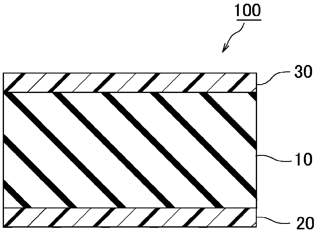
Adhesive tape

A technology of adhesive tape and adhesive layer, applied in the direction of adhesive types, ester copolymer adhesives, polymer adhesive additives, etc., can solve the problem of increased adhesive force, adhesive residue on adherends, There are no problems such as no effect, and the effects of suppressing residual glue, suppressing the increase of adhesive force, and easy handling are achieved.

Active Publication Date: 2018-12-11
NITTO DENKO CORP
View PDF6 Cites 0 Cited by
  • Summary
  • Abstract
  • Description
  • Claims
  • Application Information

AI Technical Summary

Problems solved by technology

[0005] However, when a conventional adhesive tape for dicing is used for laser dicing, the following problems arise: the adhesive force of the adhesive tape for dicing increases significantly after laser dicing, and subsequent processing (for example, cutting semiconductor elements into small pieces) removal, or transfer to another adhesive tape, etc.) becomes difficult, and adhesive residue occurs on the removed adherend
However, through this kind of response, it still has no effect on eliminating the above-mentioned phenomenon.

Method used


Image

  • Adhesive tape
  • Adhesive tape
  • Adhesive tape

Examples


Embodiment

[0123] Hereinafter, the present invention will be specifically described by way of examples, but the present invention is not limited by these examples. Unless otherwise specified, parts mean parts by weight, and % means % by weight. In addition, the amount of the reagent supplied in the form of a solution is represented by the amount of solid content remaining after volatilizing the solution (solid content conversion amount).

[0124]

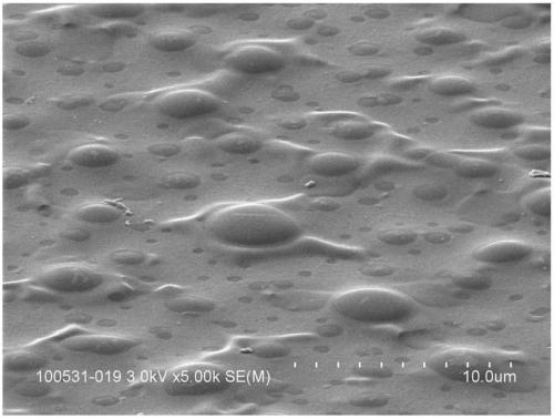
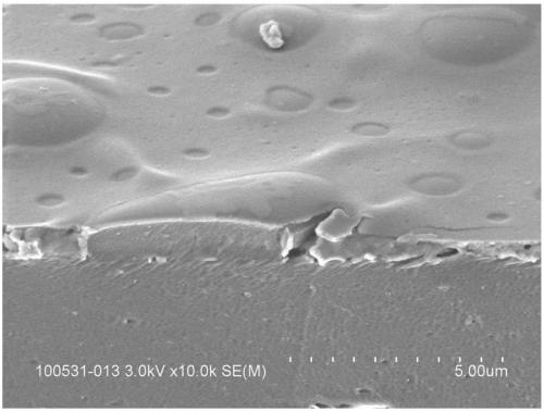
[0125] An indentation test was performed on the surface of the pressure-sensitive adhesive layer under the following conditions, and the indentation hardness and indentation modulus of elasticity were determined from the results.

[0126] (Measurement device and measurement conditions)

[0127] Device: Tribo Indenter manufactured by Hysitron Inc.

[0128] Indenter used: Berkovich (triangular cone type)

[0129] Measurement method: single indentation measurement

[0130] Measuring temperature: 25°C, 100°C

[0131] Indentation depth setti...

manufacture example 1

[0167] [Manufacturing example 1]: Manufacture of base material

[0168] Manufactured by calendaring method Contains 27 parts by weight of DOP plasticizer (bis(2-ethylhexyl phthalate), manufactured by J-PLUS Co., Ltd.) with respect to 100 parts by weight of polyvinyl chloride with a degree of polymerization P=1050 soft polyvinyl chloride film. The thickness of the obtained flexible polyvinyl chloride film was 70 μm, the elastic modulus (MD) measured according to JIS-K-7127 (1999) was 250 MPa, and the maximum elongation measured according to JIS-K-7127 (1999) (MD) is 400%. In addition, the arithmetic mean surface roughness Ra immediately after production was 0.1 μm.

Embodiment 1

[0170] (non-adhesive layer)

[0171] 60 parts by weight of polysiloxane resin (KS-723A, manufactured by Shin-Etsu Chemical Industry), 40 parts by weight of polysiloxane resin (KS-723B, manufactured by Shin-Etsu Chemical Industry), an acrylic copolymer (methyl methacrylate ( MMA) / butyl acrylate (BA) / hydroxyethyl acrylate (HEA)=70 / 30 / 10) 50 parts by weight, tin-based catalyst (Cat-PS3, manufactured by Shin-Etsu Chemical Co., Ltd.) 10 parts by weight were mixed in a solution state, A mixed solution (1) was obtained. The mixing ratio of the polysiloxane and the (meth)acrylic polymer in the mixed solution (1) was polysiloxane:(meth)acrylic polymer=2:1 by weight ratio.

[0172] The above-mentioned mixed solution (1) was coated on one side of the soft polyvinyl chloride film obtained in Production Example 1, and dried to form a non-adhesive layer (1) having a thickness of 1.0 μm and an arithmetic mean surface roughness Ra=0.5 μm.

[0173] In addition, when the non-adhesive layer (1...


PUM

PropertyMeasurementUnit
hardnessaaaaaaaaaa
thicknessaaaaaaaaaa
thicknessaaaaaaaaaa

Abstract

The invention provides an adhesive tape which can suppress an increase of adhesive force even when being heated in laser dicing or the like, facilitates handling such as taking out of a subdivided semiconductor device and transfer to an another adhesive tape, and also prevent adhesive from remaining on an object to which the tape is applied. Provided is an adhesive tape comprising an adhesive layer at least on one side of a base material, wherein indentation hardness at 100 DEG C by a nanoindenter in the surface of the adhesive layer is 20.0 MPa or higher.

Description

[0001] This application is a divisional application of an application with an application date of April 4, 2014, an application number of 201410137377.1, and an invention title of "adhesive tape". technical field [0002] This invention relates to adhesive tapes. Background technique [0003] Semiconductor chips (chips) are produced by cutting (dicing) a semiconductor wafer on which circuits are formed. For example, by dicing a semiconductor wafer on a dicing adhesive tape, the semiconductor wafer is divided into chips (chips), and the chip is picked up from the dicing adhesive tape and used in a subsequent process (For example, refer to Patent Document 1). In this cutting process, an adhesive tape is used for the purpose of fixing the semiconductor wafer. [0004] In the conventional parting process, a cutting edge such as a rotating edge is used. However, there is a problem in that cutting chips are generated in the cutting process using the cutting edge. Therefore, in...

Claims


Application Information

Patent Timeline
Patent Type & Authority Applications(China)
IPC IPC(8): C09J7/24C09J7/30C09J133/08C09J11/06C09J11/08C09D183/04C09D133/12
CPCC09J9/00C09J133/04C09J183/04C09J2203/326C09J2433/00C09J2483/00C09J7/22C09J7/245
Inventor 由藤拓三矢田贝隆浩
Owner NITTO DENKO CORP
Why Eureka
Try Eureka