Single-layer double-sided electrode of capacitive touch screen and preparation method thereof

A capacitive touch, single-layer technology, applied in electrical digital data processing, data processing input/output process, instruments, etc., can solve problems such as reducing material costs, unable to prepare double-layer electrodes, and increasing product yield, etc. Achieve the effect of reducing etch, ensuring overlap probability and uniform distribution, and improving wetting and corrosion uniformity

Inactive Publication Date: 2018-12-11
湖南兴威新材料有限公司
View PDF5 Cites 9 Cited by
  • Summary
  • Abstract
  • Description
  • Claims
  • Application Information

AI Technical Summary

Problems solved by technology

[0007] Aiming at the above-mentioned technical problems in the related art, the present invention provides a single-layer double-sided electrode of a capacitive touch screen and a preparation method thereof, which solves the problem that the current laser etching cannot prepare double-layer

Method used


Image

  • Single-layer double-sided electrode of capacitive touch screen and preparation method thereof
  • Single-layer double-sided electrode of capacitive touch screen and preparation method thereof

Examples


Embodiment 1

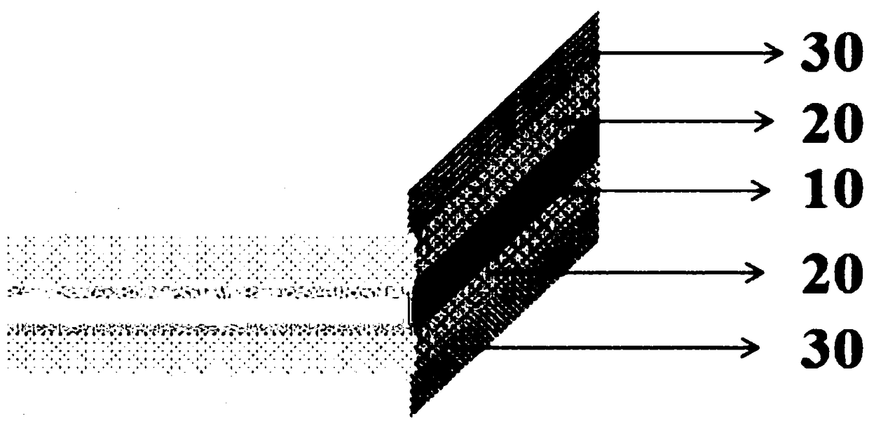
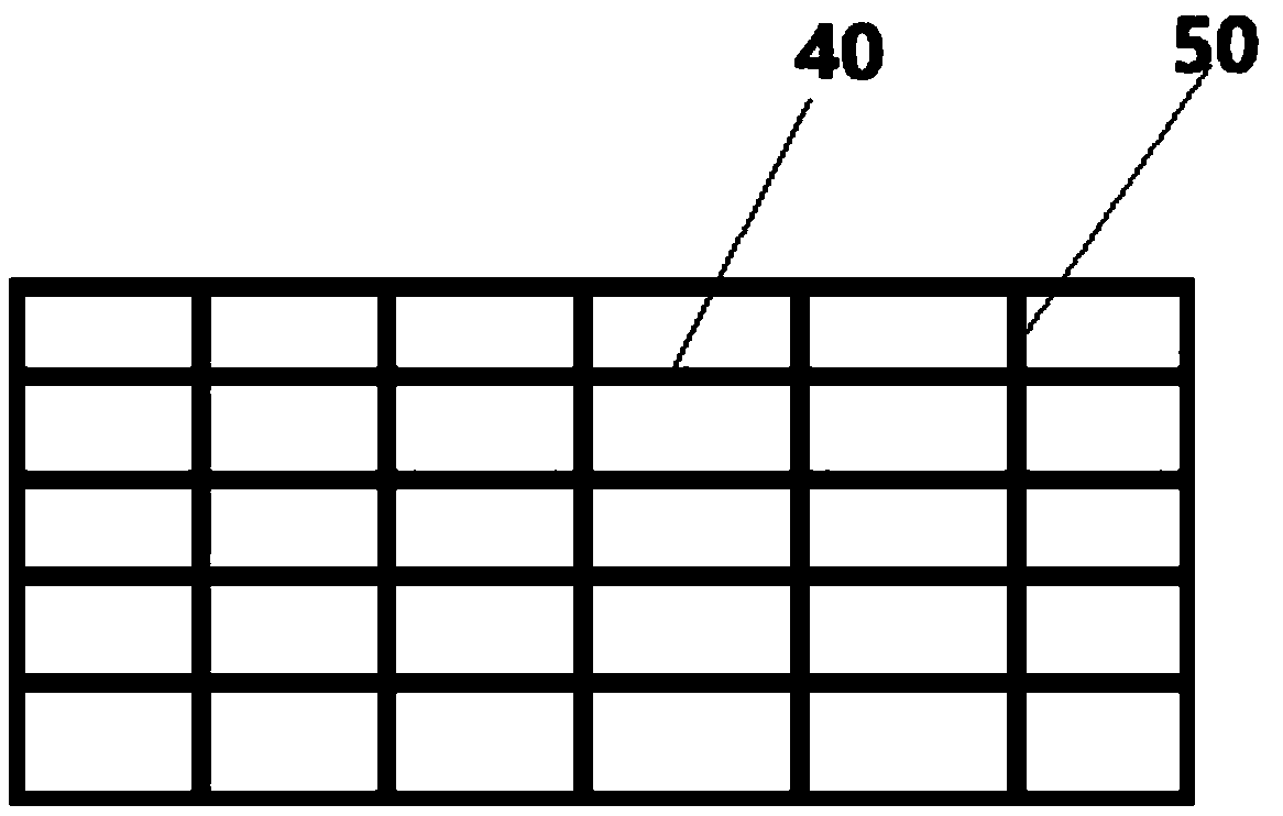
[0052] This embodiment provides a single-layer double-sided electrode of a capacitive touch screen, combined with figure 1 The schematic diagram of the layout structure shown includes a base material 10, the upper and lower surfaces of the base material are respectively provided with conductive lines, and the shown conductive lines include a silver nano wire transparent conductive layer 20 and a transparent ink layer 30 printed on the surface of the silver nano wire transparent conductive layer 20 ;Such as figure 2 As shown, wherein, the conductive lines include horizontal conductive lines 40 and vertical conductive lines 50 arranged in an array pattern arranged on different sides of the substrate 10, and the horizontal conductive lines of the single-layer double-sided electrodes in the transparent capacitive touch screen The lines 40 and the longitudinal conductive lines 50 are in a state of intersecting when viewed from above.

[0053] In this embodiment, the base film is ...

Embodiment 2

[0057] On the basis of Embodiment 1, the present invention further provides a method for preparing a single-layer double-sided electrode of a capacitive touch screen, specifically, it includes the following steps:

[0058] Step 1. Prepare nano-silver wire transparent conductive layers 20 on both sides of a PET substrate 10 with a thickness of 125 μm; bake at 100-120° C. for 5-8 minutes to prepare a double-sided silver nano-wire conductive film;

[0059] Step 2. Cut out a portion of the silver nanowire transparent conductive film obtained in step 1 that can be used to make a 21.5-inch touch screen. On one side of the silver nanowire transparent conductive layer 20, ink-jet print a transparent ink with a horizontal cell array pattern. One side is ink-jet printed with transparent ink with vertical unit array graphics. Specifically, a transparent thermoplastic resin is ink-jet printed on one side of the transparent conductive layer of silver nanowires, and an alignment point is se...

Embodiment 3

[0065] The present invention further provides a method for preparing a single-layer double-sided electrode of a large-size capacitive touch screen, specifically, it includes the following steps:

[0066] Step 1. Prepare nano-silver wire transparent conductive layers 20 on both sides of a PET substrate 10 with a thickness of 125 μm; bake at 100-120° C. for 5-8 minutes to prepare a double-sided silver nano-wire conductive film;

[0067] Step 2: Cut out a portion of the silver nano wire transparent conductive film obtained in step 1 that can be used to make a touch screen with a size of 86 inches. On one side of the silver nano wire transparent conductive layer 20, inkjet printing is provided with a transparent ink with a horizontal cell array pattern. One side is ink-jet printed with transparent ink with vertical unit array graphics. Specifically, a transparent thermosetting resin is ink-jet printed on one side of the transparent conductive layer of silver nanowires, and counter...


PUM

PropertyMeasurementUnit
Thicknessaaaaaaaaaa
Sizeaaaaaaaaaa
Thicknessaaaaaaaaaa

Abstract

The invention provides a single-layer double-sided electrode of a capacitive touch screen and a preparation method thereof. The conductive circuit comprises a silver nanowire thin film layer and a transparent ink layer printed on the surface of the silver nanowire thin film layer. The preparation process of the single-layer double-sided electrode of the capacitive touch screen is as follows: 1) preparing a nano silver wire transparent conductive film layer on the two side surfaces of the substrate; 2) printing transparent ink on that surface of the nano silver wire thin film lay to form a protective layer; 3) performing chemical etching to form a single lay double-sided electrode of that capacitive touch screen. In the electrode of the present invention, the transparent ink layer preventsthe transparent conductive layer of the silver nanowires from contacting with air. The invention effectively overcomes the problems of chemical stability deterioration and electric conductivity reduction of the nano silver wire layer caused by the phenomena of electric corrosion of the nano silver wire and silver migration, solves the problem that the double-layer electrode can not be prepared bylaser etching at present, and saves a bonding process and the use of an optical adhesive layer.

Description

technical field [0001] The invention relates to the technical field of electronic materials, in particular to a single-layer double-sided electrode of a capacitive touch screen and a preparation method thereof. Background technique [0002] Touch screen, or touch panel, is an inductive display device that can receive input signals. As the most convenient and natural input device for human-computer interaction, it is a new multimedia interactive device with a wide range of applications. With the continuous development of the electronic device market, the industry's requirements for various performances and comprehensive costs of transparent conductive materials are gradually increasing. In terms of display effect, it is difficult to meet people's increasing demand for touch screen texture and application performance, especially for large-size touch screens. Therefore, in recent years, researchers in this field expect to use a single-layer double-sided conductive film with hi...

Claims


Application Information

Patent Timeline
IPC IPC(8): G06F3/041G06F3/044
CPCG06F3/0416G06F3/044G06F2203/04103G06F2203/04112
Inventor 周剑飞黄浩张蓉
Owner 湖南兴威新材料有限公司
Why Eureka
Try Eureka