Mask substrate, mask assembly, display panel and display device
A mask substrate and display panel technology, which is applied in the direction of electrical components, electrical solid-state devices, semiconductor devices, etc., can solve problems that affect product evaporation yield and production capacity, circular edge color mixing, etc.
- Summary
- Abstract
- Description
- Claims
- Application Information
AI Technical Summary
Problems solved by technology
Method used
Image
Examples
Embodiment Construction
[0049] The following describes the embodiments of the present invention in detail, and those skilled in the art will understand that the following embodiments are intended to explain the present invention, and should not be regarded as limiting the present invention. Unless otherwise specified, in the following examples that do not explicitly describe specific techniques or conditions, those skilled in the art can carry out according to commonly used techniques or conditions in this field or according to product instructions.
[0050] In one aspect of the invention, the invention provides a mask blank.
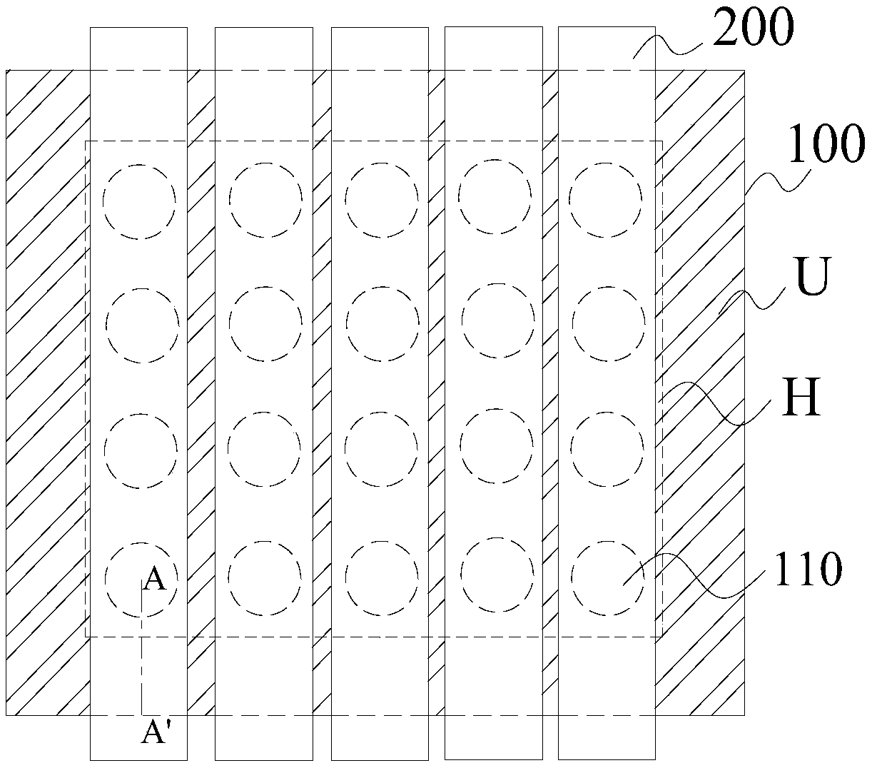
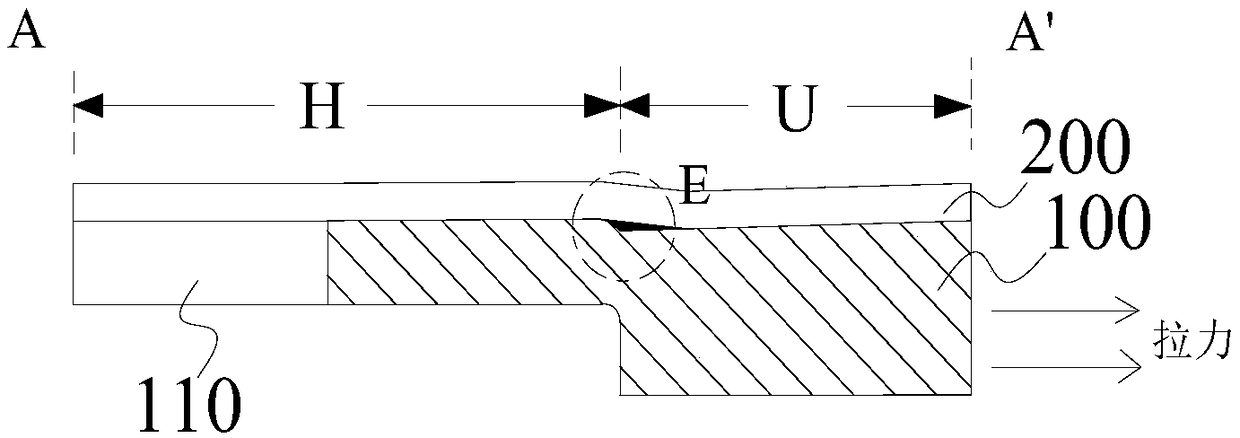
[0051] According to an embodiment of the present invention, refer to Figure 4~5, the mask substrate 100 includes a half-etched region H and a non-etched region U, the non-etched region U is arranged around the half-etched region H, and the half-etched region H has a plurality of openings 110 distributed in an array, and any one The minimum distance d′ from the opening 110 to...
PUM
 Abstract
Description
Claims
Application Information


