
A bound single-target sputtering preparation of Cu 3 sns 4 method of absorbing layer

An absorption layer and sputtering technology, which is applied in the field of Cu3SnS4 absorption layer prepared by sputtering with a single target, can solve the problems of target reduction, poor conductivity, target discharge, etc. And the effect of uniform composition and fast sputtering speed

Active Publication Date: 2020-07-31
KUNMING UNIV OF SCI & TECH
View PDF5 Cites 0 Cited by
  • Summary
  • Abstract
  • Description
  • Claims
  • Application Information

AI Technical Summary

Problems solved by technology

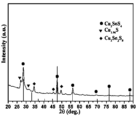
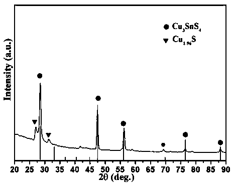
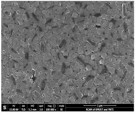
[0004] Aiming at the deficiencies of the prior art, the present invention provides a bonded single-target sputtering preparation of Cu 3 SnS 4 The method of the absorbing layer, the method of the present invention will weld the copper target and the ternary copper-tin-sulfur single target through indium, which solves the problem that the compound target is easy to form charge accumulation during sputtering due to poor conductivity, causing target discharge and cracking problem, the method of the present invention not only increases the sputtering stability of the target, but also facilitates the replacement of the target, prolongs the service life of the target, and is suitable for industrialized large-scale production; the method of the present invention is compatible with co-sputtering and sequential sputtering preparation Compared with the absorbing layer film, the number of targets is reduced, which has better controllability and greatly reduces energy consumption.

Method used


Image

  • A bound single-target sputtering preparation of Cu  <sub>3</sub> sns  <sub>4</sub> method of absorbing layer
  • A bound single-target sputtering preparation of Cu  <sub>3</sub> sns  <sub>4</sub> method of absorbing layer
  • A bound single-target sputtering preparation of Cu  <sub>3</sub> sns  <sub>4</sub> method of absorbing layer

Examples


Embodiment 1

[0026] Example 1: Preparation of Cu by sputtering with a bound single target 3 SnS 4 The method of absorbing layer, concrete steps are:

[0027] (1) Substrate pretreatment: The soda-lime glass substrate is ultrasonically cleaned with acetone, absolute ethanol, and deionized water in sequence, and the cleaned substrate is dried with nitrogen gas, and placed on a substrate rack filled with absolute ethanol For use, blow dry the substrate with nitrogen;

[0028] (2) Place the pretreated substrate in step (1) on the sample holder in the magnetron sputtering chamber, install the ternary copper-tin-sulfur target bound to the pure copper target in the magnetron sputtering chamber, adjust the binding The target base distance between the ternary copper-tin-sulfur target of the pure copper target and the substrate in the sputtering chamber is 80 mm; the ternary copper-tin-sulfur target bound to the pure copper target is the ternary copper-tin-sulfur target through The indium material...

Embodiment 2

[0033] Example 2: Preparation of Cu by sputtering with a single bound target 3 SnS 4 The method of absorbing layer, concrete steps are:

[0034] (1) Substrate pretreatment: The soda-lime glass substrate is ultrasonically cleaned with acetone, absolute ethanol, and deionized water in sequence, and the cleaned substrate is dried with nitrogen gas, and placed on a substrate rack filled with absolute ethanol For use, blow dry the substrate with nitrogen;

[0035] (2) Place the pretreated substrate in step (1) on the sample holder in the magnetron sputtering chamber, install the ternary copper-tin-sulfur target bound to the pure copper target in the magnetron sputtering chamber, adjust the binding The target base distance between the ternary copper-tin-sulfur target of the pure copper target and the substrate in the sputtering chamber is 85 mm; the ternary copper-tin-sulfur target bound to the pure copper target is the ternary copper-tin-sulfur target through The indium material...

Embodiment 3

[0042] Example 3: Preparation of Cu by sputtering with a bound single target 3 SnS 4 The method of absorbing layer, concrete steps are:

[0043] (1) Substrate pretreatment: The soda-lime glass substrate is ultrasonically cleaned with acetone, absolute ethanol, and deionized water in sequence, and the cleaned substrate is dried with nitrogen gas, and placed on a substrate rack filled with absolute ethanol For use, blow dry the substrate with nitrogen;

[0044] (2) Place the pretreated substrate in step (1) on the sample holder in the magnetron sputtering chamber, install the ternary copper-tin-sulfur target bound to the pure copper target in the magnetron sputtering chamber, adjust the binding The target base distance between the ternary copper-tin-sulfur target of the pure copper target and the substrate in the sputtering chamber is 90 mm; the ternary copper-tin-sulfur target bound to the pure copper target is the ternary copper-tin-sulfur target through The indium material...


PUM

PropertyMeasurementUnit
thicknessaaaaaaaaaa
purityaaaaaaaaaa

Abstract

The invention relates to a method for preparing Cu3SnS4 through binding-single-target sputtering, and belongs to the technical field of photoelectric film materials and new energy. The method comprises the steps of placing a pretreated substrate onto a sample shelf in a magnetron sputtering chamber, installing a ternary copper-tin-sulfur target material bound with a pure copper target into the magnetron sputtering chamber, and adjusting the target-substrate distance between the ternary copper-tin-sulfur target material bound with the pure copper target and a sputtering cavity inner substrate to be 80 to 90mm; vacuumizing the sputtering cavity inner substrate to be 2.0x10<-4> to 6.0x10<-4>Pa, and setting the working vacuum degree to be 0.4 to 0.5Pa, the substrate temperature to be 80 to 320DEG C, the sample rotating speed to be 10 to 20r / min, and the process gas flow to be 20 to 30sccm; pre-sputtering for removing impurities on the surface of the target material; adopting the ternary copper-tin-sulfur target material bound with the pure copper target to carry out direct-current sputtering on the substrate so as to deposit to form a Cu3SnS4 precursor layer thin film, wherein the sputtering power is 30 to 70w, and the thickness of the Cu3SnS4 precursor layer thin film is 790 to 810nm; and under the nitrogen environment, vulcanizing and annealing the Cu3SnS4 precursor layer thin film in excessive sulfur powder so as to obtain a Cu3SnS4 absorbing layer.

Description

technical field [0001] The invention relates to a method for preparing Cu by bound single target sputtering 3 SnS 4 The method of the absorbing layer belongs to the technical field of new energy sources of photovoltaic materials and devices. Background technique [0002] With the development of society, the non-renewability of traditional fossil energy and the environmental pollution caused by it have attracted widespread attention. For the sustainable development of human society, the development and utilization of renewable energy is becoming more and more important. The development of solar cells is one of them, CuInGaSe 2 (CIGS) and CdTe thin-film solar cells have been commercialized, but because elements such as In and Ga are rare elements in the earth's crust, and elements such as Se and Cd are toxic, the promotion and application of this type of solar cells is limited to a certain extent. As an alternative to CIGS thin film batteries, Cu 2 ZnSnS 4 (CZTS) has beco...

Claims


Application Information

Patent Timeline
Patent Type & Authority Patents(China)
IPC IPC(8): C23C14/35C23C14/06C23C14/58
CPCC23C14/0623C23C14/35C23C14/5806
Inventor 韦雷凯沈韬朱艳
Owner KUNMING UNIV OF SCI & TECH
Learn More