Coupling method for planar waveguide chip and fiber array

An optical fiber array and planar waveguide technology, which is applied in the field of optical guide communication, can solve the problems of large shrinkage of the adhesive layer, not particularly obvious changes in IL, and large fluctuation range of IL parameters, and achieves uniform thickness, thin thickness and stable optical performance. Effect

Inactive Publication Date: 2018-12-18
SICHUAN TIANYI COMHEART TELECOM
View PDF5 Cites 5 Cited by
  • Summary
  • Abstract
  • Description
  • Claims
  • Application Information

AI Technical Summary

Problems solved by technology

[0003] Coupling is an important production process of planar optical waveguide devices and AWG devices. It is a key part of product optical performance and reliability performance. Coupling process control has also become a key part of device quality. At present, FA is parallel to the coupling end face of the chip during coupling. The adhesive layer is thicker, the initial UV curing, the adhesive layer shrinks greatly, and the corresponding IL parameter fluctuation range is relatively large, and the fluctuation of IL parameter has a certain relationship with the energy of UV irradiation (only the thickness of the adhesive layer is described here), such products The aging process is not particularly pronounced for IL changes

Method used


Image

  • Coupling method for planar waveguide chip and fiber array
  • Coupling method for planar waveguide chip and fiber array

Examples


Embodiment Construction

[0018] The present invention will be further described below in conjunction with the accompanying drawings, but the protection scope of the present invention is not limited to the following description.

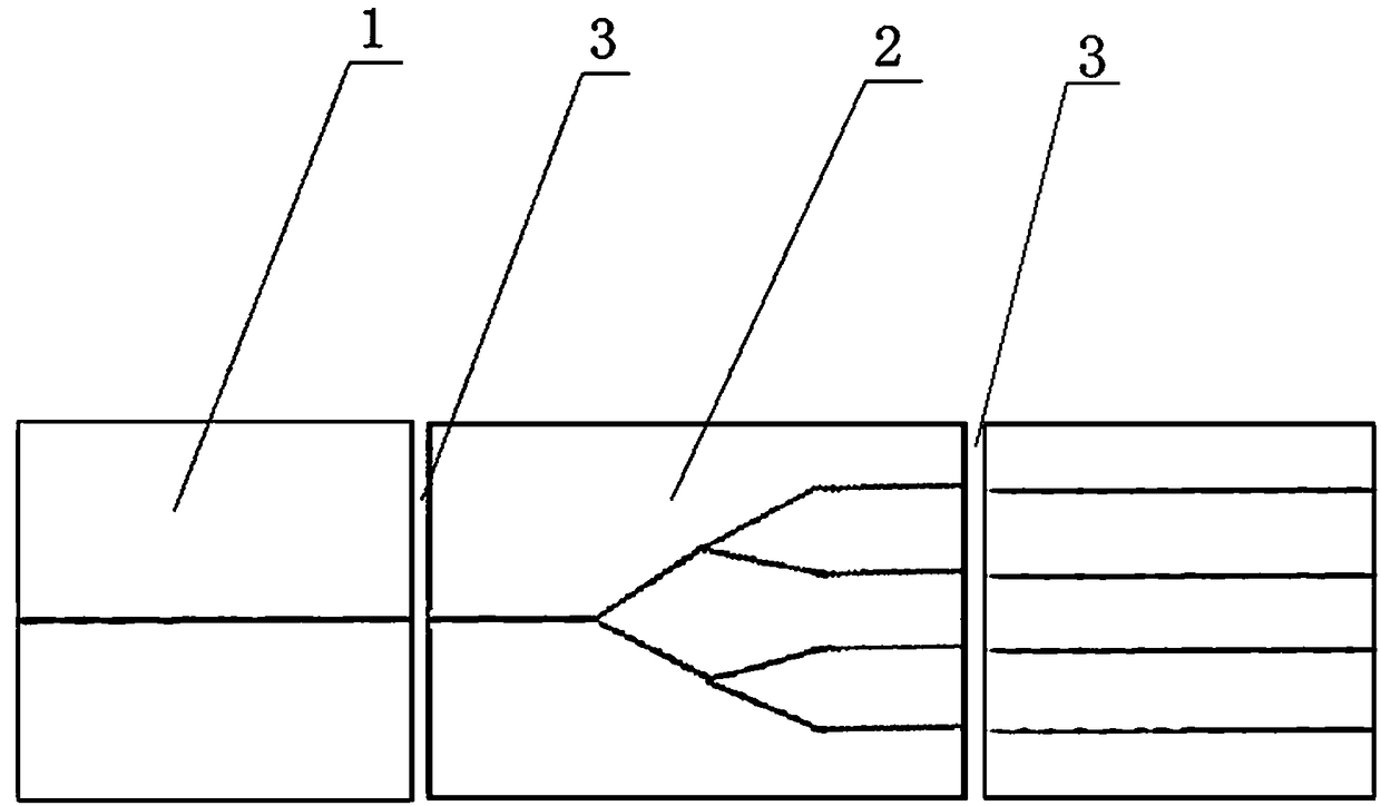
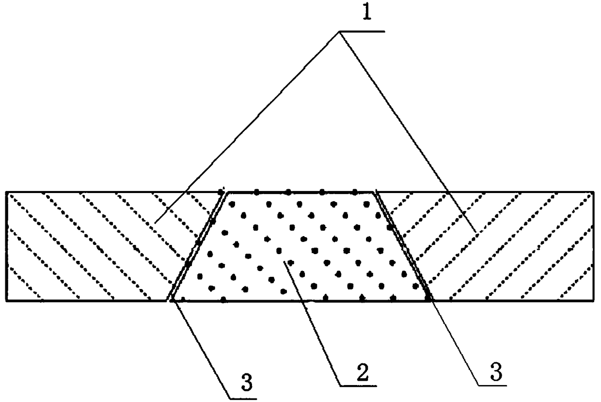
[0019] Such as Figure 1~2 As shown, a coupling method of a planar waveguide chip and an optical fiber array comprises the following steps:

[0020] S1. Clean the surface of the planar optical waveguide chip and the PLC chip, and then place the single fiber and the PLC chip on the six-dimensional adjustment frame, so that the 8° end face of the PLC chip is facing the light-transmitting surface of the FA;

[0021] S2. Adjust the six-dimensional adjustment frame to align the fiber core of the planar optical waveguide chip with the main waveguide of the input end of the PLC chip, and directly connect more than two light sources to the light source of the 2-point N optical splitter, and each station has a light source belt There are red light and wavelength light sources, and th...


PUM


Abstract

The invention discloses a coupling method for a planar waveguide chip and a fiber array. The coupling method comprises the following steps: S1, placing a single fiber and a PLC chip on a six-dimensional adjusting frame; S2, adjusting the six-dimensional adjusting frame to align a fiber core of the planar waveguide chip with a main waveguide at an input end of the PLC chip, and completing aligned light transmission of a 1CH / 2CH fiber array and a display waveguide chip through a red light derived image; S3, adjusting the six-dimensional adjusting frame to make an output end of the PLC chip parallel to an 8-degree end face of the fiber array until no gap exists between display contact surfaces of a horizontal CCD and a vertical CCD, and adjusting the product attenuation value of an optical power meter to lowest; and S4, gluing left and right 8-degree end faces of the planar optical waveguide chip, the fiber array and the PLC chip, so that glue on a dispensing surface can flow evenly to the 8-degree end faces. The coupling method has the advantage that the thickness of a coupling adhesive layer can be controlled within 10 microns, and the 8-degree end faces are evenly coated.

Description

technical field [0001] The invention relates to the field of light guide communication, in particular to a coupling method of a planar waveguide chip and an optical fiber array. Background technique [0002] With the rapid development of broadband communication network based on optical fiber network and the popularization of triple play, optical distribution network (ODN) is a key part of optical access network, which is composed of optical splitter, optical fiber cable and optical distribution products Composition, in which the optical splitter is the core device in the ODN. Today, the main factors affecting optical splitters are external mechanical shock and the influence of the environment on the optical performance of the product. The reliability of mechanical shock through raw materials and process control is relatively stable. As the demand for optical splitters increases, it is of great significance to increase the life of optical splitters and reduce the variation o...

Claims


Application Information

Patent Timeline
Patent Type & Authority Applications(China)
IPC IPC(8): G02B6/30
Inventor 袁春英何芯锐高小燕
Owner SICHUAN TIANYI COMHEART TELECOM
Why Eureka
Try Eureka