
Preparation method of 99.6 percent of Al2O3 ceramic substrate for thin film integrated circuit

A technology for ceramic substrates and integrated circuits, applied in circuits, semiconductor/solid-state device manufacturing, electrical components, etc., can solve the problems of high cost, expensive equipment, complex technology, etc., achieve smooth surface, extremely thin and uniform thickness, softening high point effect

Active Publication Date: 2017-07-28
CHINA ZHENHUA GRP YUNKE ELECTRONICS
View PDF6 Cites 1 Cited by
  • Summary
  • Abstract
  • Description
  • Claims
  • Application Information

AI Technical Summary

Problems solved by technology

Although chemical mechanical polishing can reduce the surface roughness of the substrate, due to the high hardness of the alumina substrate, the roughness after polishing can only reach 0.04-0.05μm, the mirror effect is not obvious, and the polishing liquid consumed is more costly High, long polishing time and low efficiency. According to the statistics of experiments, one piece of 99.6% Al is polished 2 o 3 The time of the ceramic substrate is more than 2h
At the same time, although there is also a method of depositing a thin film on the surface of the substrate by using special technical means in the prior art, the existing method requires expensive equipment, complicated technology and high cost, and is not suitable for actual production applications.
[0005] Therefore, the surface treatment process and performance indicators of the existing alumina ceramic substrates are difficult to meet the application requirements of high-performance thin film devices / circuits. Requirements for substrates with high reliability, low cost, and high appearance quality

Method used


Image

  • Preparation method of 99.6 percent of Al2O3 ceramic substrate for thin film integrated circuit
  • Preparation method of 99.6 percent of Al2O3 ceramic substrate for thin film integrated circuit
  • Preparation method of 99.6 percent of Al2O3 ceramic substrate for thin film integrated circuit

Examples


preparation example Construction

[0045] In view of the shortcomings of the existing alumina ceramic substrates in terms of performance and preparation technology, relevant researchers in the field of alumina ceramic substrates have conducted in-depth research on the surface treatment of substrates. In addition to polishing, there are also surface treatment methods. Coating method, coating technology mainly includes chemical vapor deposition (CVD), physical vapor deposition (PVD), thermal spraying method, screen printing method, sol-gel method, etc. With the development of modern ceramic glaze technology, glass glaze technology It has been applied to the preparation of insulating layers and the packaging of electronic devices. Glass glaze is a thin layer of uniform vitreous substance fused on the surface of the substrate. It has the characteristics of smooth and bright, high mechanical strength, stable chemical properties, and good matching with the substrate. There are very few reports on coating high-tempera...

Embodiment 1

[0081] (1) ingredients, mixing

[0082] Raw material according to 99.6% Al 2 o 3 -0.3%MgO-0.1%SiO 2 The mass ratio is carried out batching, and the mixed material that has weighed, agate ball, deionized water are put into the ball mill in the agate jar according to the ratio of 1:2:1 and mix;

[0083] Ball milling parameters are: 387rpm, 6h. After ball milling, pour out the slurry, put it in an oven at a constant temperature of 90°C for 48 hours, and pass through a 100-mesh screen;

[0084] (2) Configuration cast material

[0085] adding organic solvent ethanol and toluene, and binder PVB to the alumina powder obtained after drying and sieving to obtain a cast material;

[0086] (3) Casting and lamination

[0087] Using the tape casting method, the casting material is passed through the casting machine to obtain alumina green ceramic tape, the film thickness of which is 59±1μm, and then stacked, the number of layers is 9, and then isostatic pressing and cutting processes ...

Embodiment 2

[0108] Change the composition of the glass: according to the basic formula, in CaO-Al 2 o 3 -SiO 2 Change the composition and content of additives in the glass phase formation interval, as shown in the following table:

[0109] Table 3 Modified glass formula design

[0110]

[0111] Then put the ingredients into the corundum crucible of the frit furnace, and melt in the high-temperature frit furnace to form glass. The melting temperature is changed to 1500°C, and the holding time is 1h. After melting, it was poured into deionized water for quenching treatment to obtain a colorless and transparent glass body. Prepare glass slurry after ball milling, and then evenly spin-coat the glass slurry on the surface of the substrate by means of glue homogenization, and then perform heat treatment. The heat treatment temperature is changed to 1250° C., and other process conditions remain unchanged.

[0112] The heat-treated substrate has a high surface finish and a mirror effect, w...


PUM

PropertyMeasurementUnit
Thicknessaaaaaaaaaa
Roughnessaaaaaaaaaa
Melting pointaaaaaaaaaa

Abstract

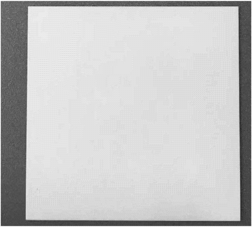
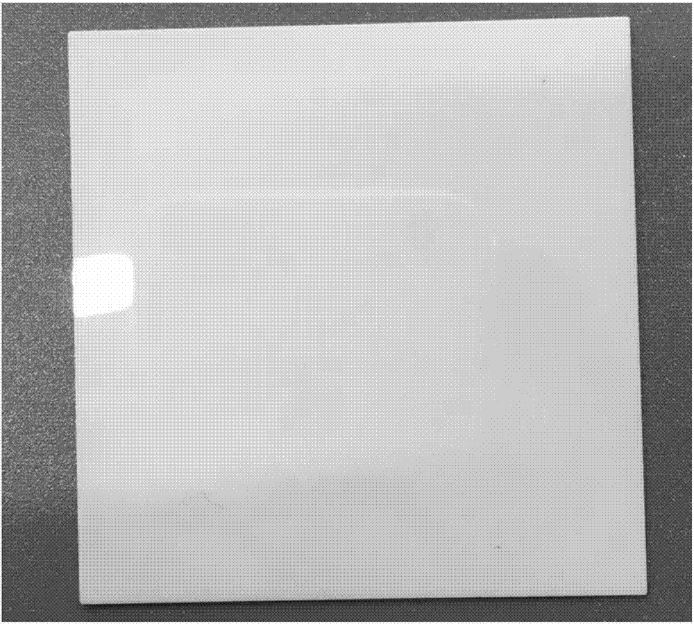
The invention provides a preparation method of a 99.6% Al2O3 ceramic substrate for a thin film integrated circuit. Through the preparation method of the 99.6% Al2O3 ceramic substrate for the thin film integrated circuit, provided by the invention, the surface roughness of the substrate can be reduced, so that the smoothness and the flatness are improved, therefore, the precision and the reliability of the thin film integrated circuit are improved, and the practical value is important. Meanwhile, the preparation method of the 99.6% Al2O3 ceramic substrate for the thin film integrated circuit, provided by the invention, has the advantages of being small in surface roughness, good in flatness, good in smoothness, specular in surface and the like.

Description

technical field [0001] The invention relates to the field of microwave dielectric ceramic substrates for thin film hybrid integrated circuits, in particular to 99.6% Al substrates for thin film integrated circuits 2 o 3 Preparation method of ceramic substrate. Background technique [0002] 99.6%Al 2 o 3 Electronic ceramic substrates have the advantages of high temperature resistance, high electrical insulation performance, low dielectric loss, high thermal conductivity, strong chemical stability, and similar thermal expansion coefficients to components, so they are widely used in thick / thin film hybrid integrated circuits and various in thin film components. [0003] However, due to the high hardness and large grains of the 99.6% alumina ceramic substrate, the surface finish of the substrate after processing is difficult to achieve a mirror effect (<0.02 μm). Even if the ceramic substrate is mechanically thinned and polished, there are still micron The thin film circ...

Claims


Application Information

Patent Timeline
IPC IPC(8): C04B41/85C04B35/10C03C12/00C03C6/04H01L21/84
CPCC03C1/00C03C12/00C04B35/10C04B41/009C04B41/5022C04B41/85C04B2235/3206C04B2235/3418H01L21/84C04B41/4539C04B41/0072
Inventor 居奎庞锦标班秀峰窦占明杨康杨俊韩玉成
Owner CHINA ZHENHUA GRP YUNKE ELECTRONICS
Learn More