A PCB type TVS diode package and a preparation process thereof

A preparation process and diode technology, which is applied in semiconductor/solid-state device manufacturing, electrical components, electric solid-state devices, etc. It can solve the problems of different thermal expansion coefficients of metal and epoxy rubber cakes, limit the number of single pieces, and break welding wires, etc. , to achieve high air tightness, save space and reduce gaps

Pending Publication Date: 2018-12-18
SHAOXING IN CONJUNCTION WITH THE ELECTRONICS TECH
View PDF0 Cites 2 Cited by
  • Summary
  • Abstract
  • Description
  • Claims
  • Application Information

AI Technical Summary

Problems solved by technology

[0003] The purpose of the present invention is to provide a PCB-type TVS diode package and its preparation process to solve the current process limitations proposed in the above background technology. The number of single chips is small, the UPH is very low during production, and a large amount of production equipment needs to be invested to increase production capacity. ;At the same time, the thermal expansion coefficients of metal and epoxy rubber cakes are different. When welding and using on the market, it is prone to cracking and penetration. At the same time, there is also the problem of internal stress expansion and breaking of welding wires.

Method used


Image

  • A PCB type TVS diode package and a preparation process thereof
  • A PCB type TVS diode package and a preparation process thereof
  • A PCB type TVS diode package and a preparation process thereof

Examples


Embodiment Construction

[0034] The following will clearly and completely describe the technical solutions in the embodiments of the present invention with reference to the accompanying drawings in the embodiments of the present invention. Obviously, the described embodiments are only some, not all, embodiments of the present invention. Based on the embodiments of the present invention, all other embodiments obtained by persons of ordinary skill in the art without making creative efforts belong to the protection scope of the present invention.

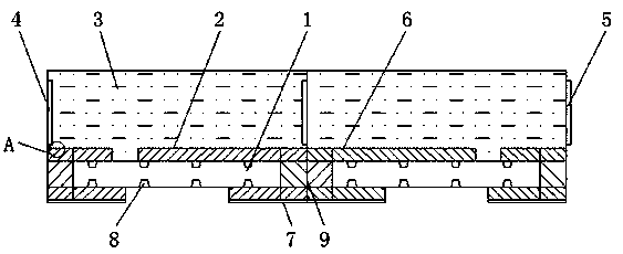
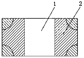
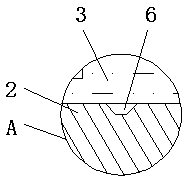
[0035] see Figure 1-3 , the present invention provides a technical solution: a PCB type TVS diode package and its preparation process, including BT resin PCB board 1 and epoxy resin 3, the outer surface of BT resin PCB board 1 is provided with TVS tube 2, epoxy resin 3 is placed on the upper surface of the TVS tube 2, the left end surface of the epoxy resin 3 is provided with a matching groove 4, and the right end surface of the epoxy resin 3 is fixed with a ...


PUM


Abstract

The invention discloses a PCB type TVS diode package and a preparation process thereof, comprising a BT resin PCB board and an epoxy resin, wherein the outer surface of the BT resin PCB board is provided with a TVS tube, and the epoxy resin is arranged on the upper surface of the TVS tube. A BT resin (bismaleimide (BMI) and triazine-based resin) is use as a substrate for that PCB positive and negative sides of the package and the preparation proces of the PCB-type TVS diode, and an etching line is used as a conduction, the substrate replaces a metal frame, and then the process flow is taken asa solid crystal, a bonding line, a stamping die, a cutting, a testing, a braiding and a warehousing; BT resin has a very high adhesion to the external sealant (epoxy resin) when molding, It is much higher than the combination with the metal frame, so that the product has higher air tightness, meanwhile, the expansion coefficient is close when the metal frame is heated and expanded, and the internal stress is smaller, so as to avoid the breakage problem of the metal frame when the metal frame is welded at the client end, and the product has higher reliability and quality.

Description

technical field [0001] The invention relates to the technical field of TVS diode packaging, in particular to a PCB type TVS diode packaging and a preparation process thereof. Background technique [0002] Transient voltage suppressor diode, referred to as TVS diode, is a high-efficiency protection device in the form of a diode. When the two poles of the TVS diode are impacted by reverse transient high energy, it can The magnitude of square seconds) makes its impedance drop suddenly, and at the same time absorbs a large current, clamping the voltage between its two ends at a predetermined value, so as to ensure that the subsequent circuit components are not damaged by the impact of transient high energy. At present, the packaging of conventional TVS diodes belongs to semiconductor packaging. In the production process, its production process is: die bonding, welding, compression molding, T / F (trimming / bending) molding, baking, testing, tape, and storage ; The specific steps a...

Claims


Application Information

Patent Timeline
Patent Type & Authority Applications(China)
IPC IPC(8): H01L23/495H01L29/861H01L21/329
CPCH01L23/49562H01L23/49575H01L23/49586H01L29/6609H01L29/861
Inventor 窦鑫
Owner SHAOXING IN CONJUNCTION WITH THE ELECTRONICS TECH
Why Eureka
Try Eureka