A GaN-based insulated gate bipolar transistor and a processing method thereof

A technology of bipolar transistors and insulated gates, applied in semiconductor devices, semiconductor/solid-state device manufacturing, electrical components, etc., can solve the problems of increasing device manufacturing process difficulty and manufacturing cost, and achieve elimination of tailing current and reduction of shutdown Power consumption, the effect of improving device yield

Active Publication Date: 2018-12-18
SOUTHEAST UNIV
View PDF4 Cites 0 Cited by
  • Summary
  • Abstract
  • Description
  • Claims
  • Application Information

AI Technical Summary

Problems solved by technology

However, the above-mentioned structures will increase the difficulty and cost of the device manufacturing process, so it is not the best way to solve the problem.

Method used


Image

  • A GaN-based insulated gate bipolar transistor and a processing method thereof
  • A GaN-based insulated gate bipolar transistor and a processing method thereof
  • A GaN-based insulated gate bipolar transistor and a processing method thereof

Examples


Embodiment Construction

[0029] In order to make the technical problems, technical solutions and beneficial effects solved by the present invention clearer, the present invention will be further described in detail below in conjunction with the embodiments and accompanying drawings. It should be understood that the embodiments described here are only used to specifically explain the present invention, and are not used to limit the scope of the claims of the present invention.

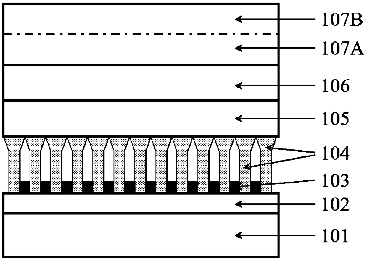
[0030] Such as figure 1 As shown, it is a GaN-based insulated gate bipolar transistor provided by the present invention, and its chip structure includes a substrate (101), a GaN or AlN buffer layer (102), and a SiN mask layer (103) arranged in sequence from bottom to top. ), GaN columnar layer (104), GaN collector region (105), N-type Al 0.2 Ga 0.8 N buffer layer (106), GaN drift region (107A), MOS structure region (107B).

[0031] First, a GaN buffer layer (102) with a thickness of 100 nm is epitaxially grown on the sapphi...


PUM

PropertyMeasurementUnit
Thicknessaaaaaaaaaa

Abstract

The invention discloses a GaN-based insulated gate bipolar transistor and a processing method thereof. The chip structure thereof comprises a substrate, a GaN or AlN buffer layer, a mask layer, a GaNpillar layer, a GaN collector region, an N-type Al<x>Ga<1-x>N buffer layer, GaN drift region and MOS structure region. The mask layer can trigger the epitaxial growth mode of GaN to change from two-dimensional planar growth to columnar growth, which is helpful to eliminate the stress caused by the mismatch between GaN and substrate and improve the crystal quality of GaN epitaxial layer. It can also realize the stripping process from the GaN columnar layer, which greatly reduces the fragmentation probability and greatly improves the yield of the device. The N-type Al<x>Ga<1-x>N buffer layer isintroduced, which effectively eliminates trailing currents during device turn-off and improves device performance with relatively small thickness. The processing method is of great significance to preparing GaN-based insulated gate bipolar transistors with high yield, low cost and low turn-off power dissipation.

Description

technical field [0001] The invention relates to a power semiconductor electronic device and a processing method thereof, in particular to a GaN-based insulating gate bipolar transistor and a processing method thereof. Background technique [0002] Compared with Si, GaAs and other materials of the first and second-generation semiconductors, the third-generation semiconductor materials represented by GaN have larger forbidden band width, higher breakdown voltage and good radiation resistance and high temperature resistance. , so it is one of the most potential materials used in the fields of high voltage, high frequency, high temperature and high power devices. [0003] At present, GaN-based insulated gate bipolar transistors are mostly prepared based on GaN substrates. However, due to the characteristics of its device structure, after completing part of the device process, the substrate with a thickness of hundreds of microns needs to be thinned to about 100 microns or even ...

Claims


Application Information

Patent Timeline
IPC IPC(8): H01L29/739H01L29/06H01L21/78H01L21/331
CPCH01L21/7813H01L29/0684H01L29/66325H01L29/7394
Inventor 张雄赵见国崔一平
Owner SOUTHEAST UNIV
Why Eureka
Try Eureka