Method for manufacturing InP monolithic microwave integrated circuit

A microwave integrated circuit and indium phosphide single-chip technology, which is applied in the field of indium phosphide materials, can solve problems such as fragmentation and damage in the production process, and achieve the effects of improving the processing yield, no surface scratches, and avoiding corrosion defects

Active Publication Date: 2012-06-20
INST OF MICROELECTRONICS CHINESE ACAD OF SCI
View PDF6 Cites 6 Cited by
  • Summary
  • Abstract
  • Description
  • Claims
  • Application Information

AI Technical Summary

Problems solved by technology

[0006] In order to achieve the above object, the main purpose of the present invention is to provide a method for making InP MMIC, to solve the problem of fragmentation caused by the fragile physical properties of InP that often occurs in the MMIC

Method used


Image

  • Method for manufacturing InP monolithic microwave integrated circuit
  • Method for manufacturing InP monolithic microwave integrated circuit
  • Method for manufacturing InP monolithic microwave integrated circuit

Examples


Example Embodiment

[0038] In order to make the objectives, technical solutions, and advantages of the present invention clearer, the following further describes the present invention in detail in conjunction with specific embodiments and with reference to the accompanying drawings.
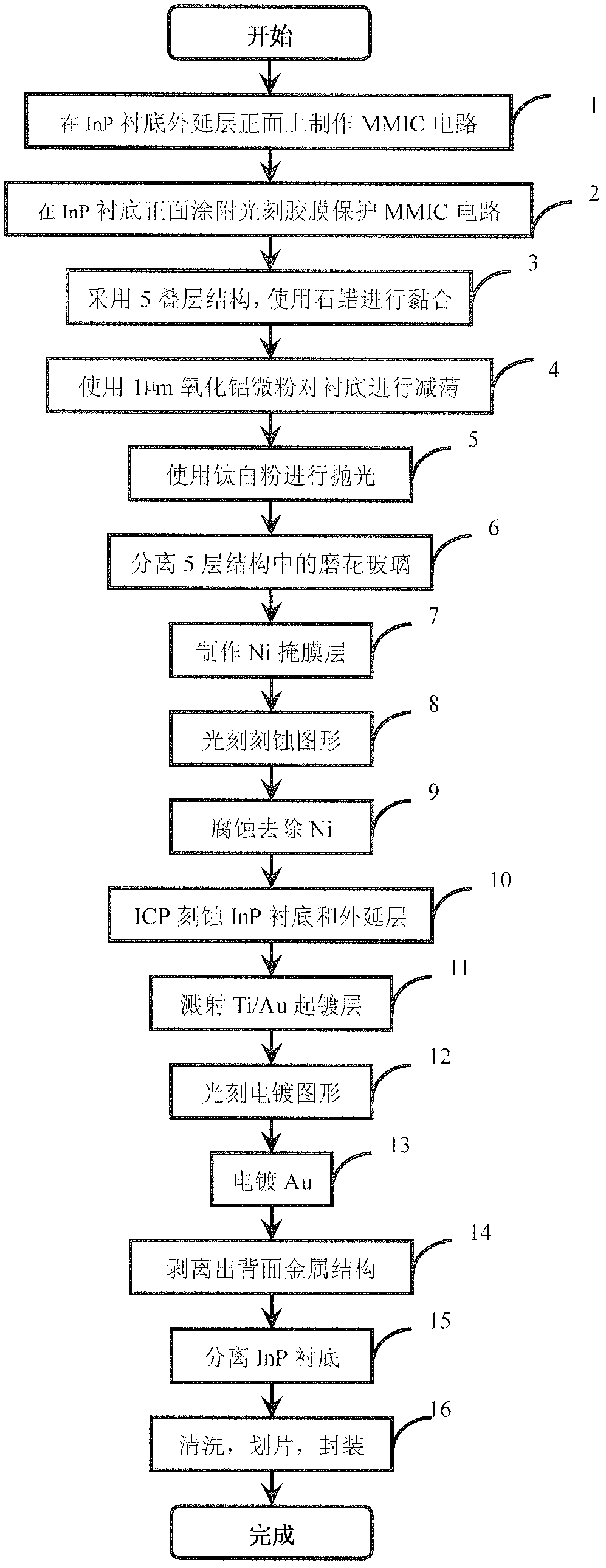
[0039] Such as figure 1 As shown, figure 1 It is a flow chart of a method for making InP MMIC according to an embodiment of the present invention, including the following steps:
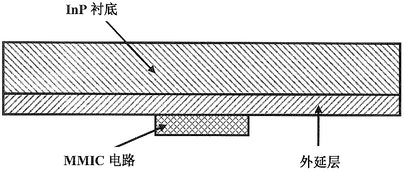
[0040] Step 1: Fabricate an MMIC circuit on the epitaxial layer on the front of the InP substrate, including: front die unit structure, wiring, air bridge structure, capacitor, resistance matching network, etc.

[0041] Step 2: Coating a photoresist layer on the epitaxial layer on the front surface of the InP substrate and the MMIC circuit to protect the MMIC circuit to form an InP substrate.
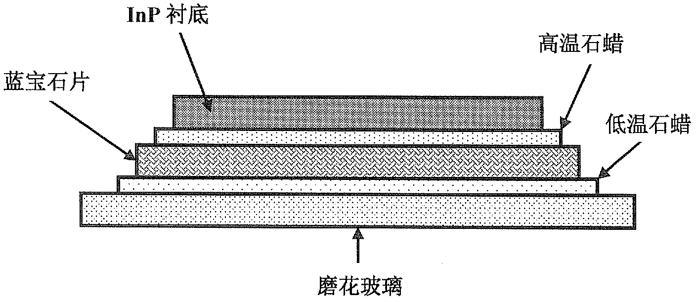
[0042] Step 3: Use paraffin waxes with different melting points and different flexibility to bond the InP substrate, the sapphire double-sided polishing she...


PUM

PropertyMeasurementUnit
Thicknessaaaaaaaaaa
Etching depthaaaaaaaaaa
Thicknessaaaaaaaaaa

Abstract

The invention discloses a method for manufacturing an InP monolithic microwave integrated circuit. The method comprises the following steps: an MMIC (Monolithic Microwave Integrated Circuit) is manufactured on an epitaxial layer on the front side of an InP underlay; a photoresist layer is coated to protect the MMIC, and an InP substrate is formed; the InP substrate, a sapphire double-sided polishing piece and a polished glass substrate are adhered by adopting paraffin to form a five-layer laminating structure; the back side of the InP substrate in the five-layer laminating structure is abraded, attenuated and polished; an Ni mask layer is manufactured on the polished surface of the back side of the InP substrate; part of the Ni mask layer is removed by utilizing the corrosion of HF acid; an HBr gas is used to etch the back side of the InP substrate, the InP underlay and the epitaxial layer on the front side of the InP underlay are etched to the MMIC circuit on the epitaxial layer; a Ti/Au coating is sputtered on the Ni mask layer; Au is electroplated on the Ti/Au coating; Au outside the Ti/Au coating is stripped by ultrasound to obtain a back-side metal structure; the high-temperature paraffin is thawed, and the sapphire double-sided polishing piece in the five-layer laminating structure is separated.

Description

technical field [0001] The invention relates to the technical field of indium phosphide (InP) materials, in particular to a method for manufacturing an indium phosphide monolithic microwave integrated circuit (InP MMIC). Background technique [0002] With the continuous application of high technology in the military field, the frequency of radio frequency microwave signals is getting higher and higher, the frequency band is getting wider and wider, and the processing capability of digital chips is getting stronger and stronger. Modern warfare has gradually entered the information age and digital age. With its excellent frequency characteristics, III-V compound semiconductor devices and related ultra-high-speed digital / digital-analog hybrid circuits are becoming the core of modern defense equipment such as military communications, radar, guidance, space defense, high-speed intelligent weapons and electronic countermeasures One of the components. Especially in the field of te...

Claims


Application Information

Patent Timeline
IPC IPC(8): H01L21/8252H01L21/02H01L21/768
Inventor 汪宁王显泰苏永波郭建楠金智
Owner INST OF MICROELECTRONICS CHINESE ACAD OF SCI
Why Eureka
Try Eureka