Flexible touch panel and preparation method thereof
A flexible touch and flexible substrate technology, applied in the direction of instruments, electrical digital data processing, data processing input/output process, etc., can solve the problems of cracking of the touch layer, increase of resistivity, decrease of hardness, etc.
- Summary
- Abstract
- Description
- Claims
- Application Information
AI Technical Summary
Problems solved by technology
Method used
Image
Examples
preparation example Construction
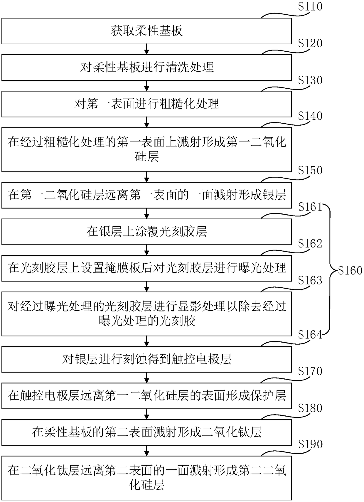
[0034] see figure 1 , the preparation method of the flexible touch panel of an embodiment, comprises the following steps:
[0035] S110. Acquire a flexible substrate.
[0036] In one embodiment, the material of the flexible substrate is selected from at least one of polyethylene terephthalate (PET) and polyimide (PI).
[0037] In one embodiment, the thickness of the flexible substrate is 0.01mm˜0.5mm. Further, the thickness of the flexible substrate may also be 0.05mm, 0.1mm or 0.25mm.
[0038] Wherein, the flexible substrate has a first surface and a second surface opposite to the first surface.
[0039] S120, cleaning the flexible substrate.
[0040] In one embodiment, when cleaning the flexible substrate, the flexible substrate is firstly scrubbed, and then the scrubbed flexible substrate is sequentially put into water and alcohol for ultrasonic cleaning. Further, water is deionized water.
[0041] In one embodiment, after the flexible substrate is ultrasonically clea...
Embodiment 1
[0094] The flexible touch panel of this embodiment is prepared by the following method:
[0095] (1) Obtain a flexible substrate with a thickness of 0.1 mm. The flexible substrate is a polyethylene terephthalate substrate. The substrate is dried in alcohol vapor.
[0096] (2) Roughen the first surface of the flexible substrate by reactive ion etching until the roughness of the first surface is 30.1nm, and the power of reactive ion etching is 60W for roughening. in CF 4 and O 2 Under the mixed gas atmosphere, CF 4 The gas flow rate is 250sccm, O 2 The gas flow rate is 200 sccm, and the roughening treatment time is 3 minutes.
[0097] (3) The first silicon dioxide layer is formed by sputtering on the first surface by magnetron sputtering, the power of magnetron sputtering is 750W, the rate of magnetron sputtering is 25nm / min, and the flow rate of oxygen is 10sccm , the flow rate of argon gas is 600 sccm, the target base distance of magnetron sputtering is 8 cm, and the thi...
Embodiment 2
[0103] The flexible touch panel of this embodiment is prepared by the following method:
[0104] (1) Obtain a flexible substrate with a thickness of 0.1 mm. The flexible substrate is a polyethylene terephthalate substrate. The substrate is dried in alcohol vapor.
[0105] (2) The first surface of the flexible substrate is roughened by reactive ion etching until the roughness of the first surface is 33nm. The power of reactive ion etching is 75W when roughening. in CF 4 and O 2 Under the mixed gas atmosphere, CF 4 The gas flow rate is 300sccm, O 2 The gas flow rate is 100 sccm, and the roughening treatment time is 3 minutes.
[0106] (3) The first silicon dioxide layer is formed by sputtering on the first surface by magnetron sputtering, the power of magnetron sputtering is 1000W, the rate of magnetron sputtering is 25nm / min, and the flow rate of oxygen is 15sccm , the flow rate of argon gas is 800 sccm, the target base distance of magnetron sputtering is 8 cm, and the th...
PUM
| Property | Measurement | Unit |
|---|---|---|
| thickness | aaaaa | aaaaa |
| surface roughness | aaaaa | aaaaa |
| electrical resistivity | aaaaa | aaaaa |
Abstract
Description
Claims
Application Information
 - R&D
- Intellectual Property
- Life Sciences
- Materials
- Tech Scout
- Unparalleled Data Quality
- Higher Quality Content
- 60% Fewer Hallucinations
Browse by: Latest US Patents, China's latest patents, Technical Efficacy Thesaurus, Application Domain, Technology Topic, Popular Technical Reports.
© 2025 PatSnap. All rights reserved.Legal|Privacy policy|Modern Slavery Act Transparency Statement|Sitemap|About US| Contact US: help@patsnap.com


