A double heterojunction ultraviolet detector

An ultraviolet detector and double heterojunction technology, applied in semiconductor devices, electrical components, circuits, etc., can solve problems such as the difficulty in effectively collecting photogenerated holes, achieve the effect of eliminating slow migration speed, improving quantum efficiency and response frequency

Inactive Publication Date: 2018-12-21
CHINA ELECTRONIC TECH GRP CORP NO 38 RES INST
View PDF3 Cites 13 Cited by
  • Summary
  • Abstract
  • Description
  • Claims
  • Application Information

AI Technical Summary

Problems solved by technology

[0004] The technical problem to be solved by the present invention is: it is difficult to effectively collect photogenerated holes, and a double heterojunction ultraviolet detector is provided

Method used


Image

  • A double heterojunction ultraviolet detector
  • A double heterojunction ultraviolet detector
  • A double heterojunction ultraviolet detector

Examples


Embodiment Construction

[0020] The embodiments of the present invention are described in detail below. This embodiment is implemented on the premise of the technical solution of the present invention, and detailed implementation methods and specific operating procedures are provided, but the protection scope of the present invention is not limited to the following implementation example.

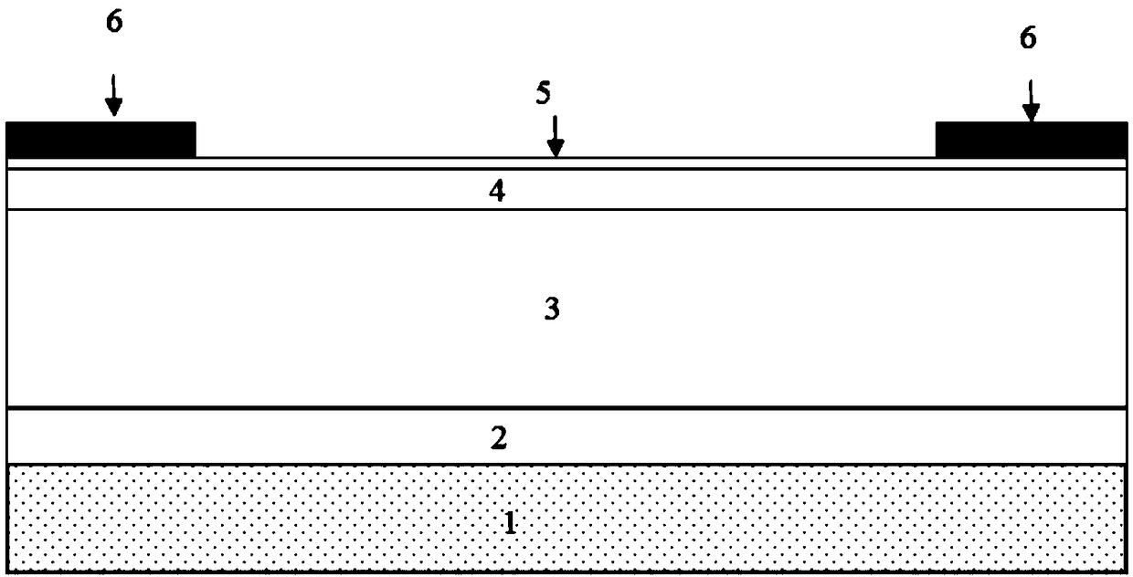
[0021] like figure 1 As shown, this embodiment includes a substrate 1, an AlN buffer layer 2, a GaN absorbing layer 3, an AlGaN barrier layer 4, a Schottky contact layer 5, and a pair of interdigitated Schottky contact layers grown epitaxially on the substrate 1 in sequence. Tertyl contact electrode 6; AlN buffer layer 2 is epitaxially grown on substrate 1, GaN absorber layer 3 is fabricated on AlN buffer layer 2, AlGaN barrier layer 4 is fabricated on GaN absorber layer 3, and Schottky contact layer 5 is fabricated On top of the AlGaN barrier layer 4 , a Schottky contact electrode 6 is formed on top of the Schott...


PUM


Abstract

The invention discloses a double heterojunction ultraviolet detector, wherein a positive polarization charge is formed on the upper surface of the GaN absorption layer and a negative polarization charge is formed on the lower surface; Under the action of the polarized charges, a two-dimensional hole gas 2DHG as a transport channel for photogenerated holes is formed between the interface of the AlNbuffer layer and the GaN absorption layer, A two-dimensional electron gas 2DEG is formed between the interface of the GaN absorption layer and the AlGaN barrier layer as a transport channel for photogenerated electrons, and the working mode of the detector is that light is incident from the upper surface of the Schottky contact layer. The invention adopts AlGaN/GaN/AlN double heterojunction to replace the traditional AlGaN/GaN single heterojunction, so that the photogenerated holes can be transported quickly through the 2DHG channel, thereby eliminating the signal tail phenomenon caused by the slow migration speed of the photogenerated holes in the single channel structure. The quantum efficiency and response frequency of the device is further improved by the efficient collection of 2DHG.Due to the existence of two-channel polarized charge, it is easier to form vertical electric field distribution in GaN absorption region.

Description

technical field [0001] The invention relates to a semiconductor optoelectronic device, in particular to a double heterojunction ultraviolet detector. Background technique [0002] Ultraviolet detection technology is another dual-use photoelectric detection technology developed after infrared and laser detection technology. Military field: The most direct application of ultraviolet detection technology is missile early warning and tracking, and ultraviolet detectors can also be used in high-security ultraviolet communication technology. Civilian fields: In medicine and biology, especially in the diagnosis of skin diseases in recent years, ultraviolet detection technology has a unique application effect. In terms of food and drug safety, ultraviolet radiation is usually used instead of chemical substances to kill microorganisms and bacteria. Therefore, ultraviolet detectors can be used to effectively monitor the disinfection of food and drug packaging, medical equipment, drin...

Claims


Application Information

Patent Timeline
Patent Type & Authority Applications(China)
IPC IPC(8): H01L31/109H01L31/0216H01L31/0304
CPCH01L31/02161H01L31/03044H01L31/109
Inventor 王俊郭进余第喜金里赵恒程国云王国胜李由
Owner CHINA ELECTRONIC TECH GRP CORP NO 38 RES INST
Why Eureka
Try Eureka