An Ingan/gan Multiple Quantum Well Structure Containing a Strain Modulated Structure

A multi-quantum well structure and quantum well layer technology, which is applied in the field of III-nitride semiconductor optoelectronic materials, can solve the problems of reduced radiation recombination efficiency, increased lattice mismatch, and misfit dislocations to eliminate stress accumulation, The effect of preventing the upward transmission of stress

Active Publication Date: 2020-04-17
TAIYUAN UNIV OF TECH
View PDF3 Cites 0 Cited by
  • Summary
  • Abstract
  • Description
  • Claims
  • Application Information

AI Technical Summary

Problems solved by technology

However, InGaN / GaN quantum wells also have inherent limitations. When the luminescent wavelength moves to the long wavelength direction, as the In composition increases, the lattice mismatch between the InGaN well layer and the GaN barrier layer increases rapidly. InGaN The rapid increase of compressive strain in the well layer leads to a strong polarization effect in the well layer and a large number of misfit dislocations
The strong polarization effect makes the energy bands of quantum wells inclined, and the wave functions of electrons and holes are separated in space, resulting in a significant decrease in the efficiency of radiative recombination, and a large number of misfit dislocations means a large number of non-radiative recombination centers
Strong polarization effects and high dislocation density greatly limit the improvement of quantum efficiency in InGaN / GaN multiple quantum wells, which also limits the performance improvement of GaN-based LEDs and lasers
In addition, the stress in the quantum well layer will pass through the GaN barrier layer upwards, causing the internal stress in the InGaN well layer to increase layer by layer, resulting in a further increase in the polarization effect and dislocation density

Method used


Image

  • An Ingan/gan Multiple Quantum Well Structure Containing a Strain Modulated Structure
  • An Ingan/gan Multiple Quantum Well Structure Containing a Strain Modulated Structure
  • An Ingan/gan Multiple Quantum Well Structure Containing a Strain Modulated Structure

Examples


Embodiment Construction

[0019] In order to make the purpose, technical solutions and advantages of the embodiments of the present invention clearer, the technical solutions in the embodiments of the present invention will be clearly and completely described below. Obviously, the described embodiments are part of the embodiments of the present invention, rather than All the embodiments; based on the embodiments of the present invention, all other embodiments obtained by persons of ordinary skill in the art without creative work all belong to the protection scope of the present invention.

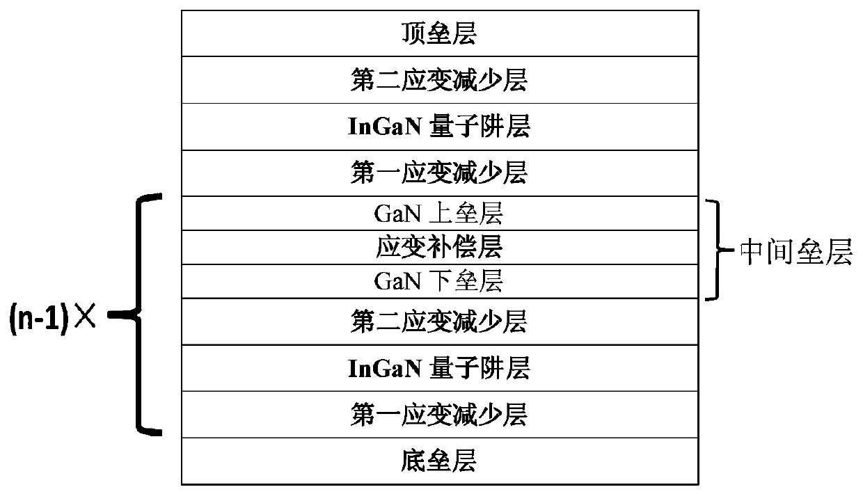
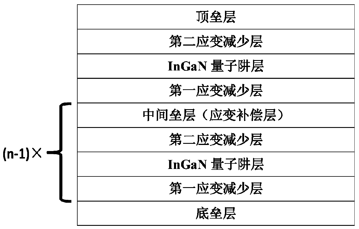
[0020] Aiming at the problems of strong polarization effect, high defect density and stress accumulation in InGaN / GaN multiple quantum wells, the present invention introduces a strain modulation structure (including strain reduction structure and strain compensation structure) in InGaN / GaN multiple quantum wells, and provides An InGaN / GaN multi-quantum well structure with a strain modulation structure provides a new ...


PUM


Abstract

The invention relates to the field of group III nitride semiconductor optoelectronic materials, An InGaN / GaN multiple quantum well structure with strain modulation structure is proposed, include an underbarrier layer, a top barrier layer, a plurality of InGaN quantum well layers located between the bottom barrier layer and the top barrier layer, and an intermediate barrier layer disposed between the respective InGaN quantum well layers, characterized by, A first strain reduction layer immediately adjacent to and disposed beneath the InGaN quantum well layer is also included, and a second strain reduction layer disposed immediately adjacent to and above the InGaN quantum well layer, The first strain reduction layer and the second strain reduction layer are InGaN layers having an In component of less than 10%, and the intermediate barrier layer comprises a strain compensation layer having a lattice constant smaller than that of the bottom barrier layer and the top barrier layer. The invention provides a novel active region structure for improving the efficiency of a GaN-based blue-green LED and a laser.

Description

technical field [0001] The invention relates to the field of Group III nitride semiconductor optoelectronic materials, in particular to an InGaN / GaN multi-quantum well structure containing a strain modulation structure. Background technique [0002] The invention of quantum well is a major breakthrough with milestone significance in the history of semiconductor material development. The concept of quantum wells began in 1963 with the double heterojunction proposed by Alferov and Cromer. Then, in 1970, using this double heterostructure, the first semiconductor laser with continuous emission at room temperature came out. In the same year, Jiang Qi and Zhu Zhaoxiang proposed the concept of superlattice. They imagined that if two kinds of materials with good lattice matching are used to alternately grow periodic structures, and the thickness of each layer of material is below 100nm, the movement of electrons along the growth direction Oscillations will be generated, which can b...

Claims


Application Information

Patent Timeline
Patent Type & Authority Patents(China)
IPC IPC(8): H01L33/12H01L33/32
CPCH01L33/12H01L33/325
Inventor 贾志刚卢太平董海亮梁建马淑芳许并社
Owner TAIYUAN UNIV OF TECH
Why Eureka
Try Eureka