A multilayer ingan quantum dot structure containing a strain-modulated structure

A technology of quantum dots and quantum dot layers, applied in semiconductor devices, electrical components, circuits, etc., can solve the problems of complex strain environment of InGaN quantum dots, poor controllability of quantum dot growth, LED carrier leakage, etc., to achieve Effects of eliminating strain coupling, reducing internal strain, and eliminating strain accumulation

Active Publication Date: 2020-05-05
TAIYUAN UNIV OF TECH
View PDF10 Cites 0 Cited by
  • Summary
  • Abstract
  • Description
  • Claims
  • Application Information

AI Technical Summary

Problems solved by technology

[0005] Although InGaN quantum dots have inherent structural advantages, there is also a more complex strain environment, which makes the growth controllability of quantum dots worse.
Although the low density of states can reduce the threshold current of the laser, it will also lead to insufficient laser gain and the problem of LED carrier leakage.
[0006] Therefore, it is necessary to propose a new multilayer InGaN quantum dot structure to solve the complex strain environment and low density of states of InGaN quantum dots in the prior art.

Method used


Image

  • A multilayer ingan quantum dot structure containing a strain-modulated structure
  • A multilayer ingan quantum dot structure containing a strain-modulated structure
  • A multilayer ingan quantum dot structure containing a strain-modulated structure

Examples


Embodiment Construction

[0027] In order to make the purpose, technical solutions and advantages of the embodiments of the present invention clearer, the technical solutions in the embodiments of the present invention will be clearly and completely described below. Obviously, the described embodiments are part of the embodiments of the present invention, rather than All the embodiments; based on the embodiments of the present invention, all other embodiments obtained by persons of ordinary skill in the art without creative work all belong to the protection scope of the present invention.

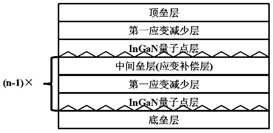
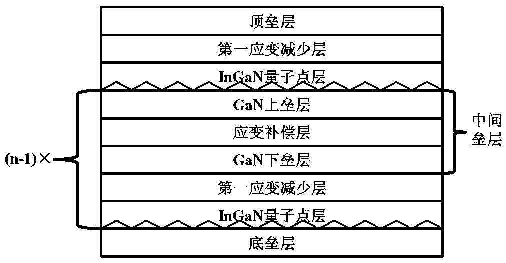
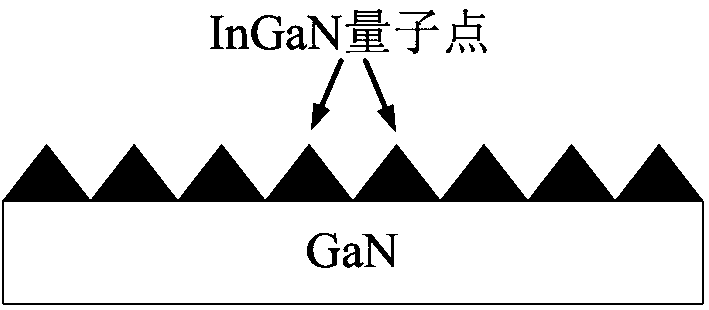
[0028] Aiming at the complex strain environment and low density of states of InGaN quantum dots, the present invention introduces a strain modulation structure (including a strain reduction structure and a strain compensation structure) into a multilayer InGaN quantum dot, and provides a multi-layered InGaN quantum dot with a strain modulation structure. The layered InGaN quantum dot structure provides a new type of ...


PUM


Abstract

The invention relates to the field of group III nitride semiconductor optoelectronic materials, and provides A multilayer InGaN quantum dot structure with a strain-modulated structure the structure includes an underbarrier lay, a top barrier layer, a plurality of InGaN quantum dot layers located between the bottom barrier layer and the top barrier layer, and an intermediate barrier layer disposedbetween the respective InGaN quantum dot layers, characterized in that it further comprises a first strain reduction layer disposed immediately adjacent to and above the InGaN quantum dot layer, wherein the first strain reduction layer is an InGaN layer having an In component of less than 10%, and the intermediate barrier layer comprises a strain compensation layer, wherein the strain compensationlayer is a barrier layer having a lattice constant smaller than that of GaN. The invention provides a novel active region structure for improving the performance of GaN-based LEDs and lasers and widening the luminous wavelength range thereof.

Description

technical field [0001] The invention relates to the field of low-dimensional structures of Group III nitrides, in particular to a multilayer InGaN quantum dot structure containing a strain modulation structure. Background technique [0002] GaN-based group III nitride materials (including AlN, AlGaN, InN, InGaN, AlGaInN) are the third generation of semiconductor materials after the first generation of silicon germanium, the second generation of gallium arsenide, and indium phosphide. The first-generation semiconductors Si and Ge are the industrial basis of modern microelectronics and integrated circuits; the second-generation GaAs and InP are the basis of red, infrared, mid-infrared and terahertz optoelectronic devices (including lasers, LEDs, detectors, etc.) Material. Group III nitrides (III-N) cover the violet, blue, green, yellow and ultraviolet bands of visible light. Among them, blue light and green light, as the three primary colors, have attracted the attention of ...

Claims


Application Information

Patent Timeline
Patent Type & Authority Patents(China)
IPC IPC(8): H01L33/06H01L33/12H01L33/32H01L33/00
CPCH01L33/0075H01L33/06H01L33/12H01L33/32
Inventor 贾志刚卢太平董海亮梁建马淑芳许并社
Owner TAIYUAN UNIV OF TECH
Why Eureka
Try Eureka