Dot matrix display device and time display device
A display device and dot matrix technology, applied to static indicators, nonlinear optics, instruments, etc., to achieve the effects of shortened forwarding time, simplified wiring structure, and low power consumption
- Summary
- Abstract
- Description
- Claims
- Application Information
AI Technical Summary
Problems solved by technology
Method used
Image

Examples
no. 1 Embodiment approach
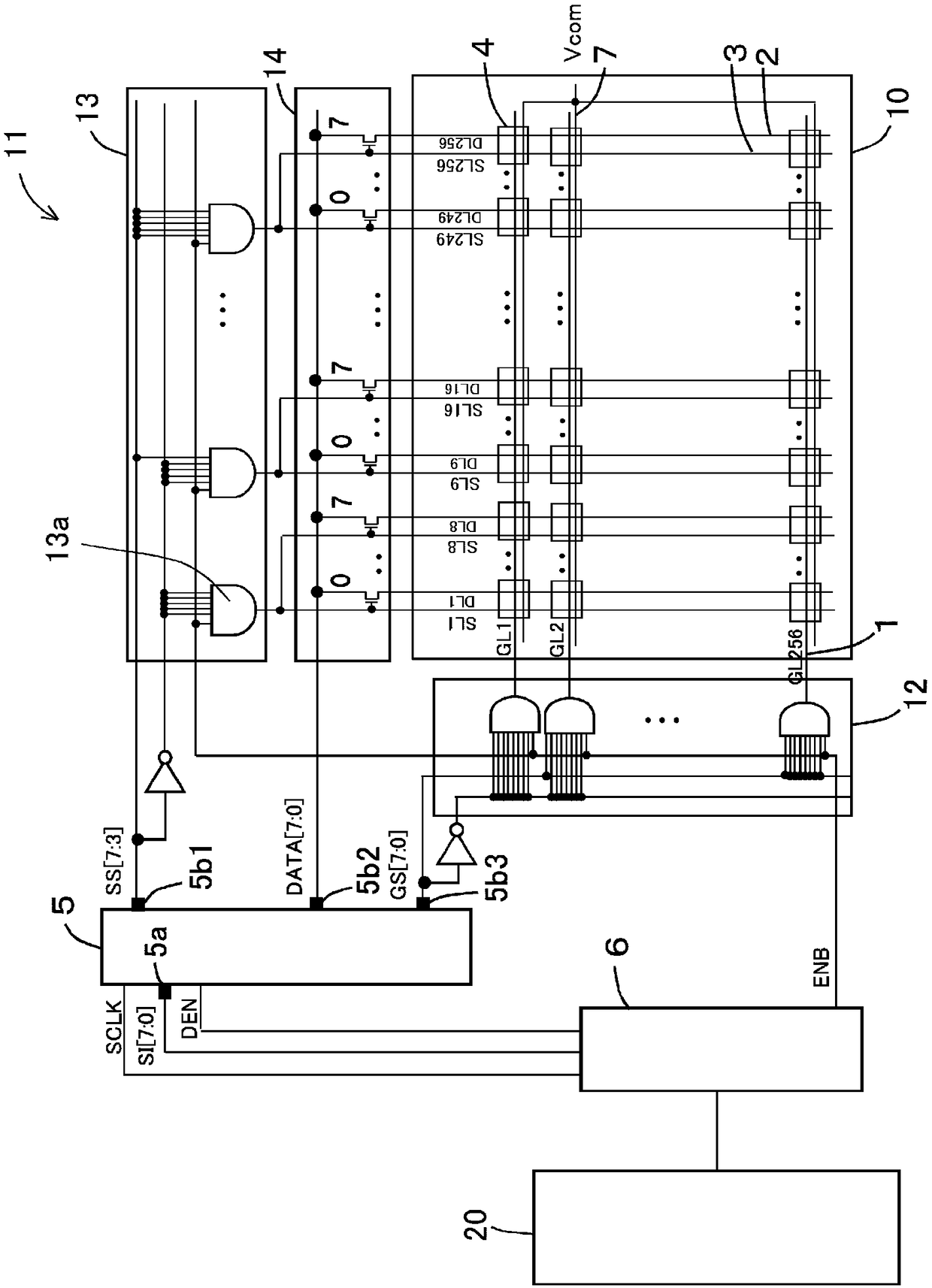
[0056] refer to Figure 1 ~ Figure 13B The dot matrix display device 11 according to this embodiment will be described. figure 1 It is a block circuit diagram showing the overall configuration of the dot-matrix display device 11 . exist figure 1 A configuration example of a dot-matrix display device 11 including a display unit 10 for black-and-white display with a pixel count of 65536 dots (256 dots in length×256 dots in width) is shown in FIG.
[0057] The dot-matrix display device 11 according to this embodiment is, for example, figure 1 As shown, it includes: a signal supply unit 6; a pixel rewriting control unit 5; a display unit 10 having pixel electrode units 4 arranged in a matrix including holding circuits (memory); direction of crossing (e.g. figure 1 The gate decoder circuit 12 of the gate signal of the gate signal line 1 (GL1 ~ GL256) arranged on the top-to-bottom direction of the top-to-bottom direction); generates a selection (set to an enabled state) in o...
no. 2 Embodiment approach
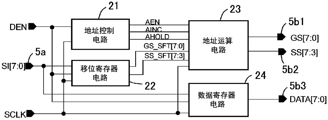
[0094] In the above-mentioned first embodiment, the general overall operation of the dot matrix display device according to the present invention was described, but in this embodiment, the drive control in the pixel rewriting control unit 5 performed in units of one pixel will be described. Case.
[0095] Figure 12A as well as Figure 12B It is a timing chart for explaining the operation of the pixel rewriting control unit 5 of the dot matrix display device 11 according to the present embodiment. which is, Figure 12A as well as Figure 12B It is a timing diagram of random access for rewriting drivers by randomly accessing addresses one by one. First, in the first cycle and the second cycle during which the data identification signal DEN is inactive, the serial signal SI[7:0] including the gate address signal and the source address signal is input from the signal supply unit 6 to the pixel rewriting control Part 5 of the shift register circuit 22. Thereafter, the data i...
no. 3 Embodiment approach
[0097] In the above-mentioned second embodiment, the case where the drive control is performed in units of one pixel is described, but in this embodiment, the case where the pixel rewriting control unit 5 is to be controlled is partially continuous is described.
[0098] Figure 13A as well as Figure 13B It is a timing chart for explaining the operation of the pixel rewriting control unit 5 of the dot matrix display device according to the present embodiment. which is, Figure 13A And 13B is a timing chart in the case of accessing consecutive addresses and performing rewriting drive. From the 1st cycle to the 3rd cycle is the same as above 12A and Figure 12B The operation is the same for the random access shown above. The gate address (GS(A)), source address (SS(B)), and image signal (DATA(A, B)) serially input in the third cycle are taken into the internal register, and rewriting is executed by The enable signal ENB of is activated, and the image data (DATA (A, B)) is ...
PUM
 Abstract
Description
Claims
Application Information
 - R&D Engineer
- R&D Manager
- IP Professional
- Industry Leading Data Capabilities
- Powerful AI technology
- Patent DNA Extraction
Browse by: Latest US Patents, China's latest patents, Technical Efficacy Thesaurus, Application Domain, Technology Topic.
© 2024 PatSnap. All rights reserved.Legal|Privacy policy|Modern Slavery Act Transparency Statement|Sitemap