
Novel ion implantation PD SOI device and preparation method therefor

A technology of ion implantation and devices, which is applied in semiconductor/solid-state device manufacturing, semiconductor devices, electrical components, etc., can solve problems such as floating body effects, achieve the effects of reducing influence, suppressing floating body effects, and avoiding chip area

Pending Publication Date: 2019-01-01
中证博芯(重庆)半导体有限公司
View PDF0 Cites 0 Cited by
  • Summary
  • Abstract
  • Description
  • Claims
  • Application Information

AI Technical Summary

Problems solved by technology

[0004] Aiming at the technical problem of floating body effect in existing N-type PD SOI devices, the present invention provides a novel ion-implanted PD SOI device, which can effectively suppress the floating body effect of PD SOI devices

Method used


Image

  • Novel ion implantation PD SOI device and preparation method therefor
  • Novel ion implantation PD SOI device and preparation method therefor
  • Novel ion implantation PD SOI device and preparation method therefor

Examples


Embodiment Construction

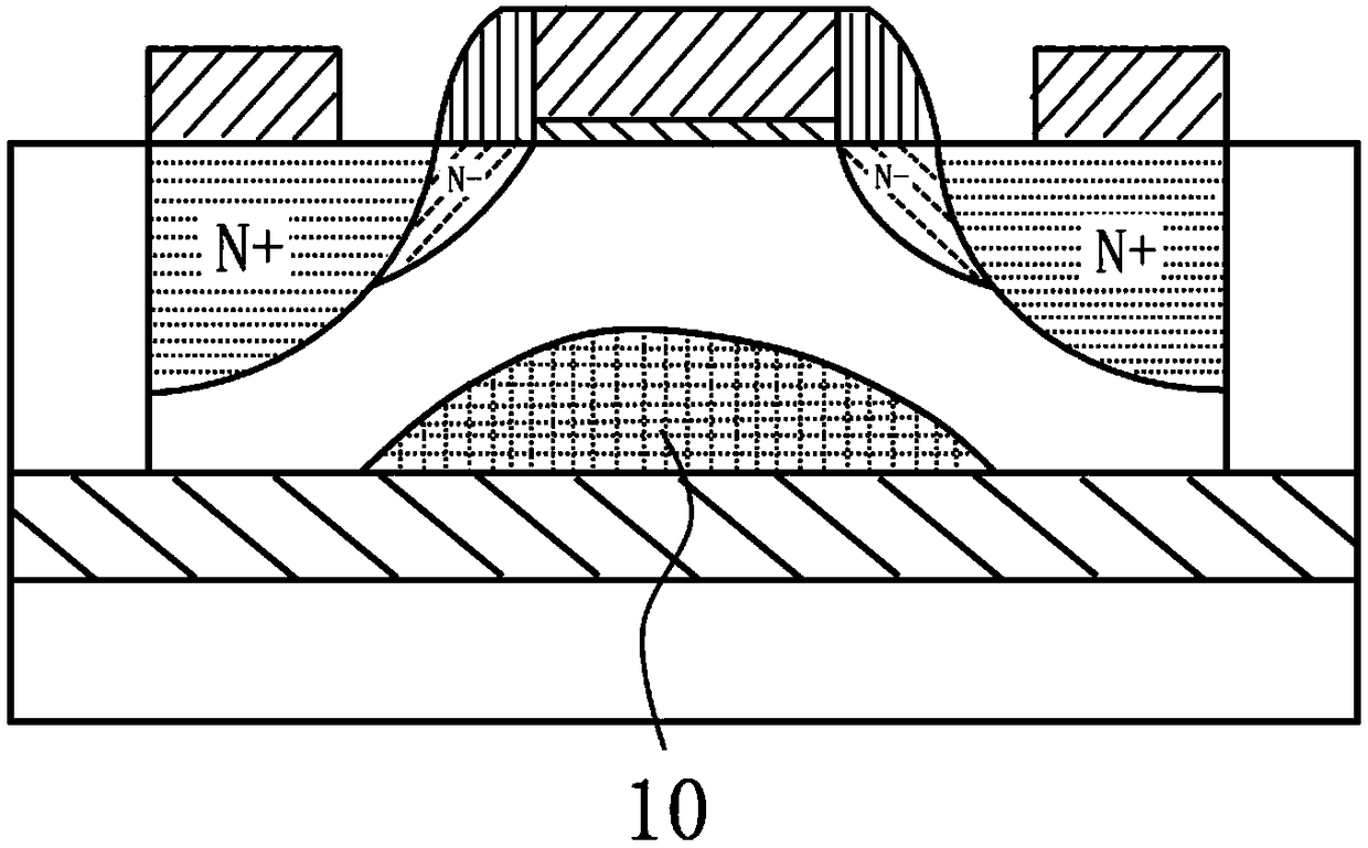
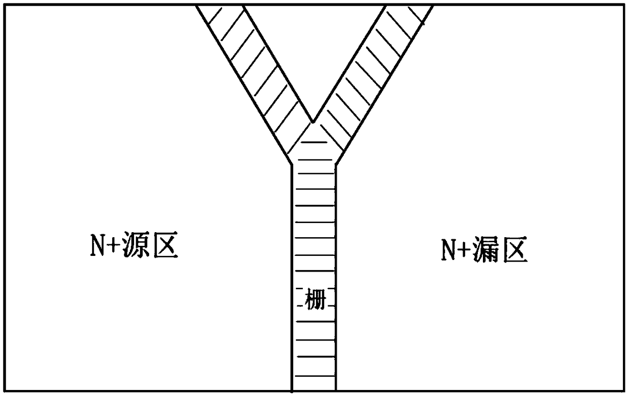
[0034]In order to make the technical means, creative features, goals and effects achieved by the present invention easy to understand, the present invention will be further described below in conjunction with specific illustrations.

[0035] In describing the present invention, it is to be understood that the terms "longitudinal", "radial", "length", "width", "thickness", "upper", "lower", "front", "rear", The orientation or positional relationship indicated by "left", "right", "vertical", "horizontal", "top", "bottom", "inner", "outer", etc. is based on the orientation or positional relationship shown in the drawings , is only for the convenience of describing the present invention and simplifying the description, but does not indicate or imply that the referred device or element must have a specific orientation, be constructed and operated in a specific orientation, and thus should not be construed as limiting the present invention. In the description of the present inventio...


PUM

PropertyMeasurementUnit
Thicknessaaaaaaaaaa
Thicknessaaaaaaaaaa
Thicknessaaaaaaaaaa

Abstract

The invention provides a novel ion implantation PD SOI device, and the device comprises an SOI substrate which is formed by the sequential overlapping of a bottom silicon layer, a central BOX buried layer and a top silicon film from the bottom to the top. Two sides of the top silicon film are provided with shallow trench isolating layers, and P ions are injected into the top silicon film to form P-type silicon. The upper surface of the top silicon film is sequentially provided with gate oxide and agate electrode, so as to form a Y-shaped distributed gate. Metal ions are injected into the top silicon film exactly below the gate to form a metal layer. Source-drain region ultra-shallow junctions are formed in the source-drain regions at two sides of the gate in a doped manner, and the periphery of the gate is provided with a gate side wall. The ion implantation is performed below the source-drain region ultra-shallow junctions to form source-drain region corona ring regions, and silicideis formed on the surfaces of the source-drain regions. The source-drain electrodes are formed on the surface of the silicide of the source-drain electrodes. The invention also provides a preparation method for the device. According to the invention, the metal ions are injected into the top silicon film to form the metal layer, thereby effectively reducing the floating effect in the PD SOI device.Moreover, the Y-shaped gate can reduce the occupied area of the chip, and increase the contact area of the gate.

Description

technical field [0001] The invention relates to the technical fields of semiconductor integrated circuits and radio frequency applications, in particular to a novel ion-implanted PD SOI device and a preparation method thereof. Background technique [0002] SOI (Silicon-on-insulator, silicon on insulator) CMOS (Complementary Metal Oxide Semiconductor, Complementary Metal Oxide Semiconductor) device is more attractive, because compared with bulk silicon CMOS device, it can completely eliminate the parasitic latch effect, and has Low power consumption, high speed, high integration and other advantages. SOI MOS devices can be divided into partially depleted SOI MOS devices (PD SOI MOS devices) and fully depleted SOI MOS devices (FD SOI MOS devices) according to the maximum depletion layer thickness. The top silicon film of the partially depleted SOI MOS device is thicker, and the body region is not completely depleted, resulting in a unique floating body effect in the device. ...

Claims


Application Information

Patent Timeline
IPC IPC(8): H01L29/06H01L29/423H01L29/78H01L21/28H01L21/336
CPCH01L29/0684H01L29/401H01L29/42356H01L29/66568H01L29/78Y02P70/50
Inventor 黄瑞周广正代京京
Owner 中证博芯(重庆)半导体有限公司
Learn More