Front face release technique of suspended microstructure

A technology of microstructure and technology, applied in the direction of microstructure technology, microstructure device, manufacturing microstructure device, etc., can solve the problems of insufficient release time, adhesion of suspended microstructure and substrate, etc., and achieve the effect of occupying a small chip area

Active Publication Date: 2017-10-20
CHINA JILIANG UNIV
View PDF7 Cites 3 Cited by
  • Summary
  • Abstract
  • Description
  • Claims
  • Application Information

AI Technical Summary

Problems solved by technology

However, if the residual stress of the microstructure is not well controlled or the release time is insufficient, it is easy to cause adhesion between the suspended microstructure and the substrate.

Method used


Image

  • Front face release technique of suspended microstructure
  • Front face release technique of suspended microstructure

Examples


Embodiment

[0026] Embodiment: Utilize the suspended microstructure front release technology provided by the present invention to manufacture an electrothermal excitation / piezoresistive detection micro-bridge resonator, and its fabrication and front release process are as follows:

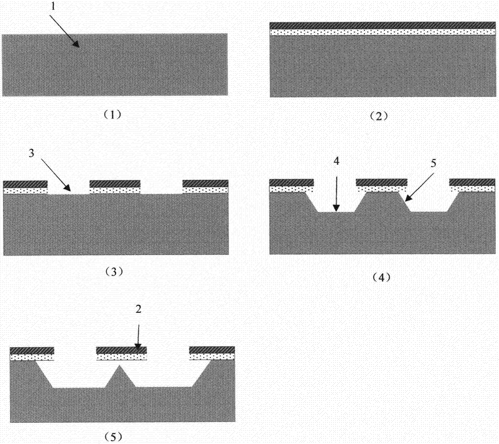
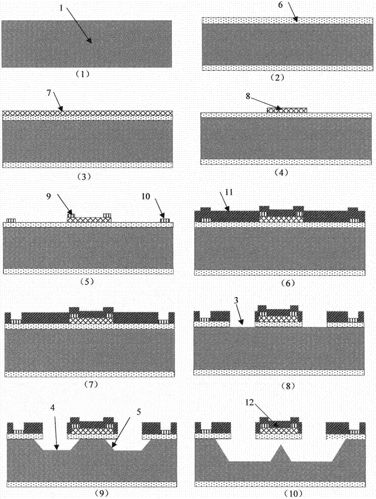
[0027] 1. The original silicon wafer is a heavily doped silicon wafer (1) with a (100) plane and a resistivity equal to 0.01Ω.cm. Standard cleaning, if attached figure 2 As shown in [1].

[0028] 2. Thermally oxidize and grow silicon dioxide film (6) at 1100°C, with a thickness of 0.6 μm, as attached figure 2 As shown in [2].

[0029] 3. Deposit polysilicon film (7) by low-pressure chemical vapor deposition method, with a thickness of 0.6 μm, as attached figure 2 Shown in [3].

[0030] 4. Ion-implanted boron, activated in a nitrogen environment at 950°C for 30 minutes, photolithographically etched the pattern of the polysilicon resistor (8), etched the polysilicon film (7) outside the resistance area, a...


PUM

PropertyMeasurementUnit
electrical resistivityaaaaaaaaaa
thicknessaaaaaaaaaa

Abstract

The invention discloses a front face release technique of a suspended microstructure. A thin film structure of a microstructure (2) is formed by using a heavily doped silicon wafer (1) as a substrate, a corrosion window (3) is formed by lithography and etching, and finally front face corrosion is performed in an anisotropic etching solution, and the microstructure (2) is cut longitudinal corroded along a surface (4) and is cut along a surface (5), so that the microstructure (2). The front face release technique of the suspended microstructure (2) requires no double-faced registration or lithography and occupies a small chip area, and the suspended microstructure (2) is not adhered with the substrate, and the design of the microstructure (2) is not limited by the crystal direction.

Description

technical field [0001] The invention relates to a front release technology of a suspended microstructure, in particular to a front release technology of a microstructure fabricated on a heavily doped silicon wafer, belonging to the field of micro-electromechanical systems (MEMS). Background technique [0002] MEMS refers to micro-devices or micro-systems such as micro-sensors, micro-mechanisms, and micro-actuators mass-produced by micro-machining technology. It raises the level of miniaturization, multi-function, intelligence and reliability of the information system to a new level. At present, MEMS products such as micro-sensors, micro-actuators, and micro-components are playing a huge role in the fields of industrial process control, communication, robotics, environmental protection and monitoring, human health, aircraft, automobile transportation, and agriculture. [0003] Micromachining technology is a means to realize various microstructures that is gradually developed...

Claims


Application Information

Patent Timeline
Patent Type & Authority Applications(China)
IPC IPC(8): B81B7/02B81C1/00
CPCB81B7/02B81B2201/0271B81C1/00055B81C1/0038B81C1/00404B81C1/00523B81C2201/0156B81C2201/0176
Inventor 韩建强韩东牛文举
Owner CHINA JILIANG UNIV
Why Eureka
Try Eureka