LDMOS device structure and manufacturing method thereof
A device structure and conductivity type technology, applied in the field of LDMOS device structure and its production, can solve problems such as device failure, affecting device service life, and threshold voltage degradation
- Summary
- Abstract
- Description
- Claims
- Application Information
AI Technical Summary
Problems solved by technology
Method used
Image

Examples
Embodiment Construction
[0022] In order to illustrate the present invention more clearly, the present invention will be further described below in conjunction with preferred embodiments and accompanying drawings. Similar parts in the figures are denoted by the same reference numerals. Those skilled in the art should understand that the content specifically described below is illustrative rather than restrictive, and should not limit the protection scope of the present invention.
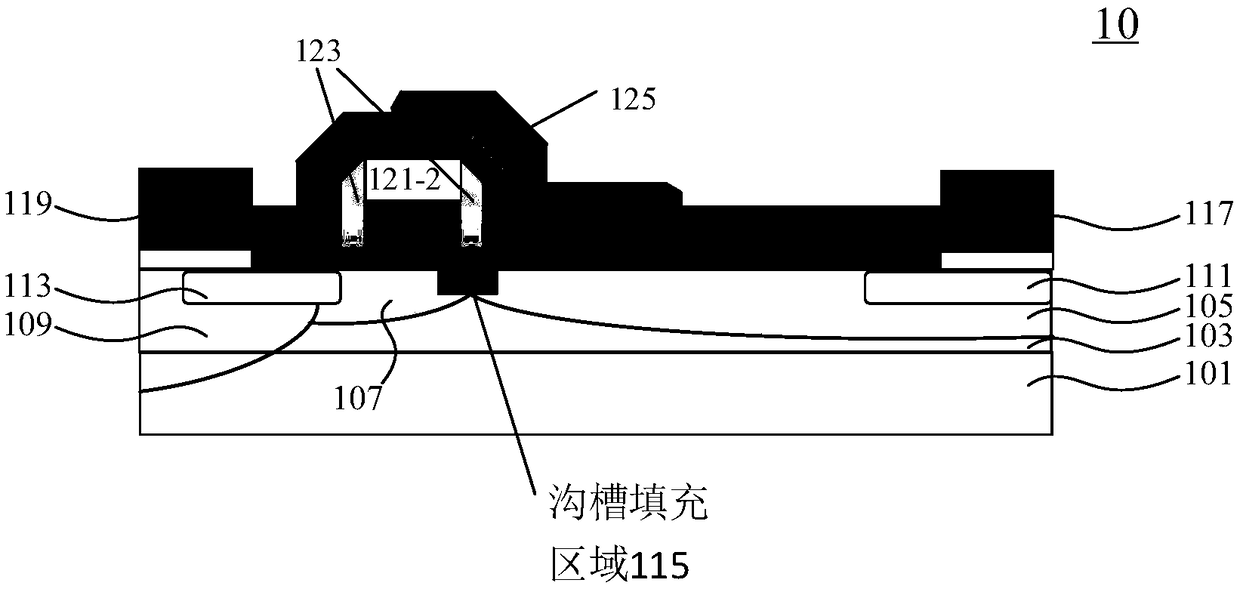
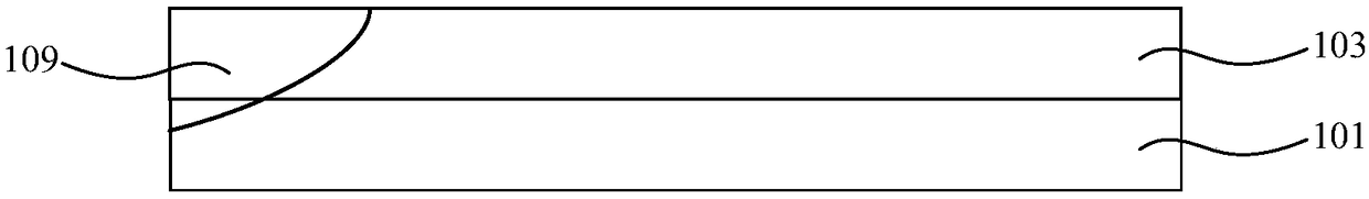
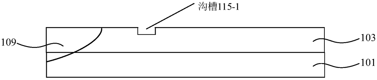
[0023] The LDMOS device structure 10 provided in this embodiment includes a substrate 101 of the first conductivity type, an epitaxial layer 103 of the first conductivity type, a lightly doped drift region 105 of the second conductivity type, and a channel region 107 of the first conductivity type. . The well region 109 of the first conductivity type, wherein the doping concentration of the substrate 101 is greater than the doping concentration of the epitaxial layer 103 . A heavily doped drain region 111 of the second con...
PUM
 Abstract
Description
Claims
Application Information
 - R&D
- Intellectual Property
- Life Sciences
- Materials
- Tech Scout
- Unparalleled Data Quality
- Higher Quality Content
- 60% Fewer Hallucinations
Browse by: Latest US Patents, China's latest patents, Technical Efficacy Thesaurus, Application Domain, Technology Topic, Popular Technical Reports.
© 2025 PatSnap. All rights reserved.Legal|Privacy policy|Modern Slavery Act Transparency Statement|Sitemap|About US| Contact US: help@patsnap.com