A silicon carbide MOSFET device and a manufacturing method thereof

A silicon carbide and device technology, which is applied in semiconductor/solid-state device manufacturing, semiconductor devices, electrical components, etc., can solve problems such as low work efficiency, high production cost, and high power loss

Active Publication Date: 2019-01-04
UNIV OF ELECTRONICS SCI & TECH OF CHINA
View PDF6 Cites 6 Cited by
  • Summary
  • Abstract
  • Description
  • Claims
  • Application Information

AI Technical Summary

Problems solved by technology

[0006] The present invention needs to be solved, that is, in view of the above problems, it proposes a device capable of optimizing the poor robustness of the device, high power loss, high power loss, etc. Silicon carbide MOSFET device with low working efficiency, high production cost and other problems and its manufacturing method

Method used


Image

  • A silicon carbide MOSFET device and a manufacturing method thereof
  • A silicon carbide MOSFET device and a manufacturing method thereof
  • A silicon carbide MOSFET device and a manufacturing method thereof

Examples


Embodiment 1

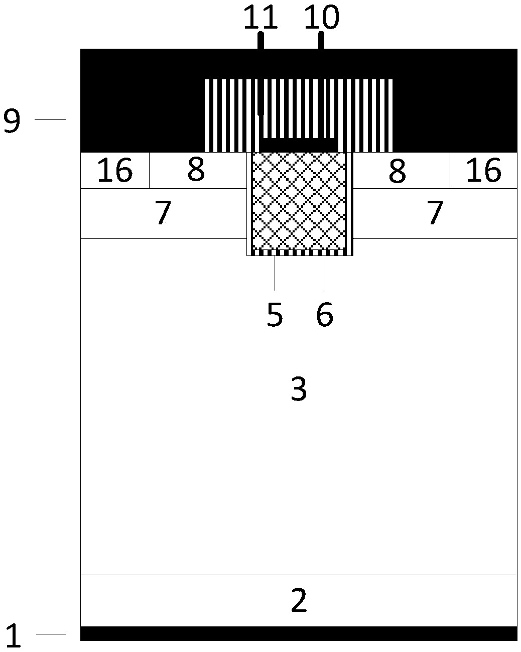
[0126] A silicon carbide MOSFET device, the cell structure of its basic structure is as follows figure 2 shown. Including drain metal 1, silicon carbide N arranged sequentially from bottom to top + Substrate 2 and SiC N - epitaxial layer 3; the silicon carbide N - There is a source trench on the upper left of the epitaxial layer 3, and the source trench is deposited and filled with Schottky contact metal 12; there is a silicon carbide deep P-doped region 4 below the Schottky contact metal 12; the Schottky contact metal 12 with SiC N - The epitaxial layer 3 is in direct contact with the sidewall at the bottom of the trench to form a Schottky contact with rectification characteristics, and the silicon carbide N - There is a silicon carbide deep P-doped region 4 on the upper right of the epitaxial layer 3, and its depth is the same as that of the silicon carbide deep P-doped region 4 below the Schottky contact metal 12; the silicon carbide N - The upper left of the silicon ...

Embodiment 2

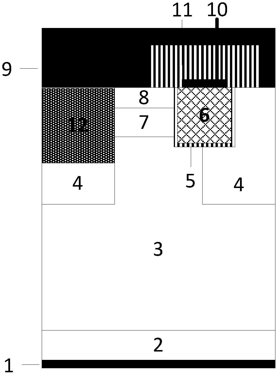
[0128] This embodiment makes a certain degree of modification to embodiment 1, and its structure is roughly the same as embodiment 1, the difference is that the Schottky contact metal 12 region used is replaced by polysilicon 13, as image 3 shown. Also, a Si / SiC heterojunction structure with a rectifying contact is formed on the bottom sidewall of the source trench and the silicon carbide N- epitaxial layer 3 . The forward conduction voltage drop Von of the heterojunction structure is about 1.1V, which also has a greater effect on the operation of the third quadrant of the device. At the same time, since the heterojunction is a multi-sub-device, the diode has good reverse recovery performance.

Embodiment 3

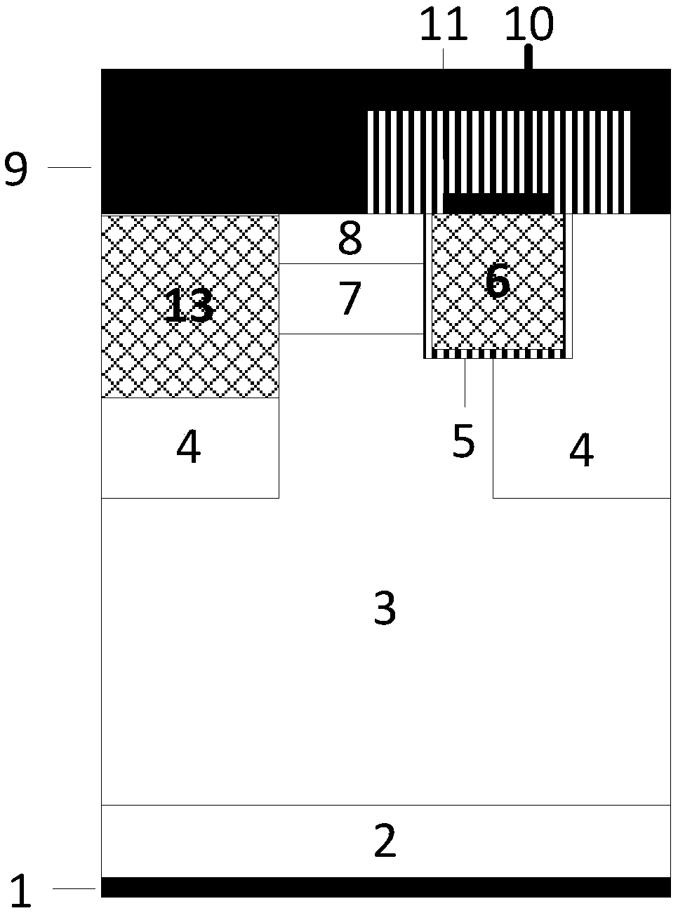
[0130] The difference between this embodiment and Embodiment 1 is that the Schottky contact metal 12 has a larger lateral dimension, such as Figure 4 As shown: the right side of the Schottky contact metal 12 exceeds the right boundary of the silicon carbide deep P-doped region 4, not only the bottom sidewall is in contact with the silicon carbide N- epitaxial layer 3, but also the bottom part of the region is in contact with the silicon carbide N - Epitaxial layer 3 contacts. The larger width of the Schottky contact metal 12 increases the contact area of ​​the Schottky junction, which has further significance for the optimization of the third quadrant of the device.


PUM

PropertyMeasurementUnit
thicknessaaaaaaaaaa
widthaaaaaaaaaa
widthaaaaaaaaaa

Abstract

The invention provides a silicon carbide MOSFET device and a manufacturing method thereof. The invention aims at a conventional silicon carbide UMOSFET structure, and proposes a multi-sub rectifier device integration mode, and includes implementation methods of Schottky contact and Si/SiC heterojunction contact. While effectively improving the basic characteristics of the traditional carbonize UMOSFET and optimizing the long-term application reliability of the device, the invention realizes the integration of the multi-sub rectifier devices, thereby greatly optimizing the work performance of the device in the third quadrant. The implementation process of the structure is compatible with the traditional silicon carbide UMOSFET process, and has the characteristic of easy fabrication.

Description

technical field [0001] The invention belongs to the power semiconductor technology, and in particular relates to a metal oxide semiconductor field effect (MOSFET) device structure and a manufacturing method thereof. Background technique [0002] Energy resources are an important material basis for human survival and development, and a source of power for human production and life. Many energy resources are inexhaustible, such as wind energy, solar energy, and tidal energy. However, the main energy used in production and life is non-renewable energy, including fossil energy, coal and natural gas, etc., which has triggered a global energy crisis. Since mankind entered the 21st century, this problem has attracted more and more attention. How to reduce unnecessary energy consumption in production and life, that is, how to improve the utilization rate of energy resources, is an important means to alleviate the global energy crisis. As one of the energy sources that can be dire...

Claims


Application Information

Patent Timeline
Patent Type & Authority Applications(China)
IPC IPC(8): H01L29/16H01L21/336H01L29/78H01L29/06
CPCH01L29/0603H01L29/1608H01L29/66477H01L29/78
Inventor 张金平邹华赵阳罗君轶李泽宏张波
Owner UNIV OF ELECTRONICS SCI & TECH OF CHINA
Why Eureka
Try Eureka