A preparation method of a back-contact heterojunction solar cell

A solar cell and heterojunction technology, applied in the field of solar cells, can solve the problems of reduced short-circuit current density, reduced carrier collection efficiency, reduced area, etc., to reduce the number of photolithography, reduce process complexity, and reduce small width effect

Active Publication Date: 2019-01-15
XIAN UNIV OF TECH
View PDF3 Cites 12 Cited by
  • Summary
  • Abstract
  • Description
  • Claims
  • Application Information

AI Technical Summary

Problems solved by technology

The large width of the isolation layer leads to a reduction in the area of ​​the P-type amorphous silicon layer and the N-type amorphous silicon layer, and the carrier collection efficiency decreases, resulting in a decrease in the short-circuit current density of the battery

Method used


Image

  • A preparation method of a back-contact heterojunction solar cell
  • A preparation method of a back-contact heterojunction solar cell

Examples


Embodiment Construction

[0032] The technical solutions in the embodiments of the present invention will be clearly and completely described below in conjunction with the accompanying drawings in the embodiments of the present invention.

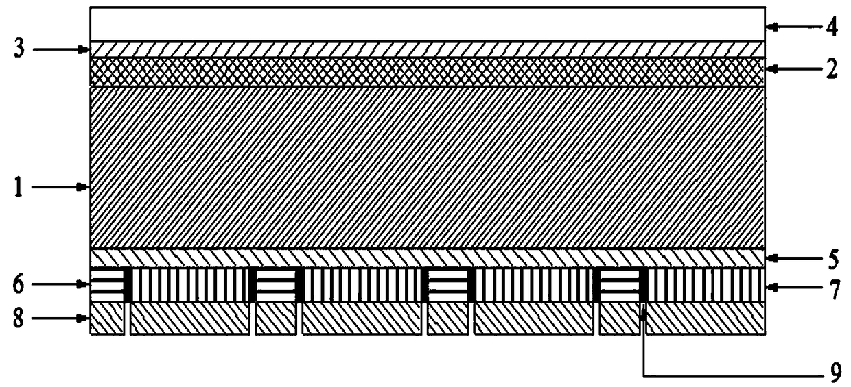
[0033] Such as figure 1 As shown, a back-contact heterojunction solar cell, taking N-type silicon as an example, includes an N-type monocrystalline silicon substrate 1, a front intrinsic amorphous silicon passivation layer 2, and a front N-type amorphous silicon layer 3. An anti-reflection layer 4, an intrinsic amorphous silicon passivation layer 5 on the back, an N-type amorphous silicon layer 6 on the back, a P-type amorphous silicon layer 7, a contact layer 8, and an insulating isolation layer 9.

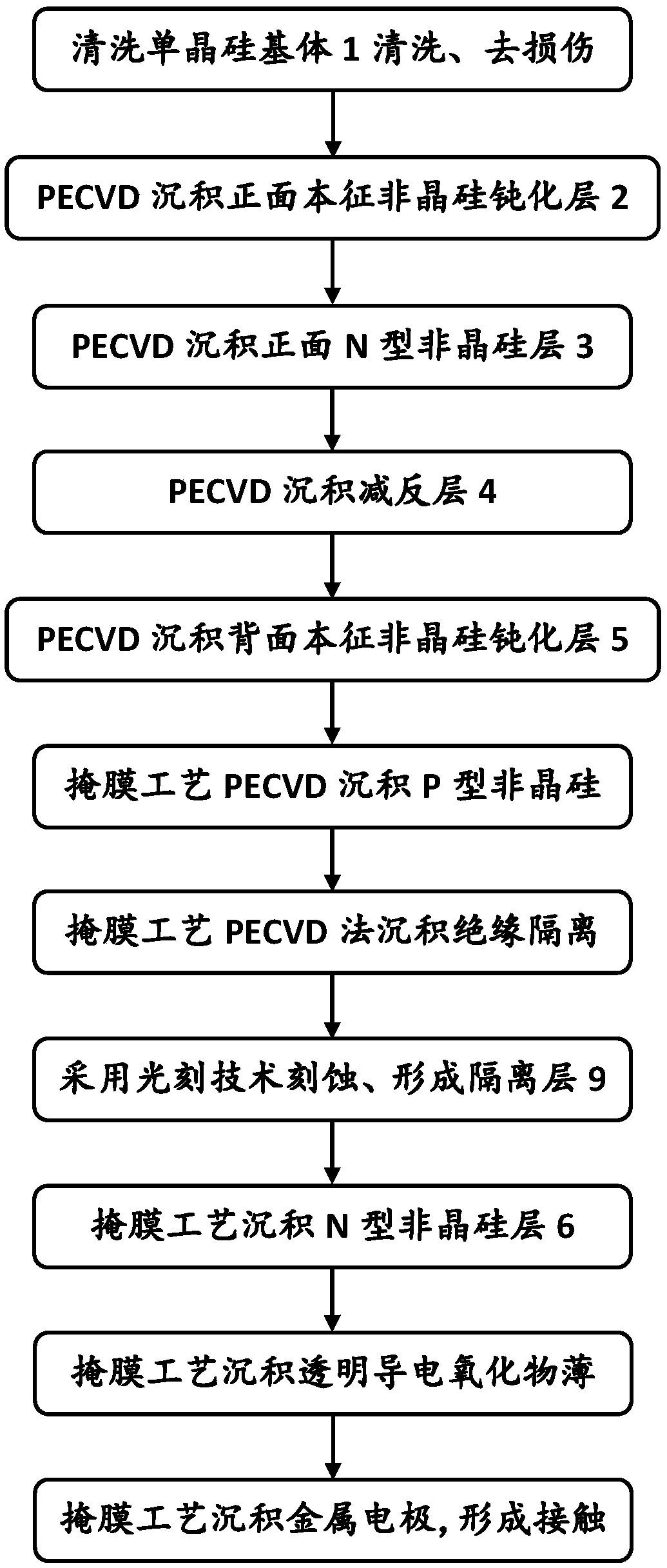
[0034] combine figure 2 The schematic diagram of the preparation method for the back of the interdigitated back-contact heterojunction solar cell is shown, and the specific implementation of the present invention is described as follows.

[0035] (a) Cleaning the mo...


PUM

PropertyMeasurementUnit
widthaaaaaaaaaa
thicknessaaaaaaaaaa
thicknessaaaaaaaaaa

Abstract

The invention discloses a preparation method of a back-contact heterojunction solar cell. A pre-passivation layer of intrinsic amorphous silicon, an N-type amorphous silicon layer and an anti-reflection layer are sequentially deposited on the front side of the washed and dedamaged layer and the velveted monocrystalline silicon substrate; Depositing an intrinsic amorphous silicon back passivation layer on the back surface of the battery; The P-type amorphous silicon layer is deposited on the surface of the back passivation layer by a mask method, and then the insulation isolation layer betweenthe P-type amorphous silicon layer and the N-type amorphous silicon layer is directly deposited, and the insulation isolation layer is etched according to the preset width of the insulation isolationlayer by a photolithography method; Further depositing an N-type amorphous silicon layer on the back surface by a mask method; At last, that transparent conductive film is sequentially deposite by adopting a mask proces, and the metal film forms a contact layer, thereby completing the preparation of the solar cell of the invention. The invention improves the preparation process precision of the back surface structure pattern of the HBC single crystal silicon solar cell, reduces the width of the isolation layer, and improves the collection probability of the photogenerated carriers and the short-circuit current density of the HBC solar cell.

Description

technical field [0001] The invention relates to the technical field of solar cells, in particular to a method for preparing an interdigitated back contact heterojunction solar cell. Background technique [0002] Interdigitated Back Contact Silicon Heterojunction Solar Cell (HBC solar cell for short) has both interdigitated back contact solar cell (Interdigitated back contact Solar Cell, IBC solar cell for short) and solar cell with The advantages of the thin intrinsic layer heterojunction solar cell (Heterojunction with Intrinsic Thin-layer Solar Cell, referred to as HIT solar cell) not only remove the metal electrode on the front surface, reduce the shading loss, obtain a large short-circuit current, but also pass Inserting a layer of high-quality intrinsic amorphous silicon passivation layer between heavily doped amorphous silicon and crystalline silicon greatly reduces the interface state, reduces surface recombination, and improves the open circuit voltage. It is current...

Claims


Application Information

Patent Timeline
Patent Type & Authority Applications(China)
IPC IPC(8): H01L31/20H01L31/068
CPCH01L31/0682H01L31/202Y02E10/547Y02P70/50
Inventor 封先锋李雨菲高萌
Owner XIAN UNIV OF TECH
Why Eureka
Try Eureka