A perovskite solar cell with specific structure and a preparation method thereof
A solar cell and perovskite technology, applied in circuits, photovoltaic power generation, electrical components, etc., can solve the problems of perovskite cell efficiency attenuation, lack of moisture resistance, and reduced efficiency, so as to increase work stability and avoid Aggravation effect, effect of improving efficiency
- Summary
- Abstract
- Description
- Claims
- Application Information
AI Technical Summary
Problems solved by technology
Method used
Image
Examples
Embodiment 1
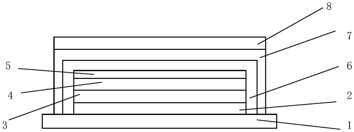
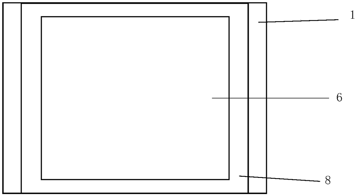
[0031] A perovskite solar cell with a specific structure, including: a conductive substrate, a metal electrode layer, an electron transport layer, a perovskite layer, a hole transport layer, a barrier / encapsulation composite layer, and a covering layer. The fabrication process is as follows:
[0032] 1) Using FTO glass as the base material, cut it into a size of 5×5cm, ultrasonically clean it with detergent solution, deionized water, and ethanol for 15 minutes each, and dry it with nitrogen flow;
[0033] 2) Spraying a dense titanium dioxide layer on the treated substrate as an electron transport layer with a thickness of 70nm;
[0034] 3) The perovskite layer was spin-coated by the anti-solvent method in a vacuum glove box, annealed at 100°C for 1 hour, and the thickness of the perovskite layer was 600nm;
[0035] 4) spin-coat the Spiro-OMeTAD hole-conducting layer in a vacuum glove box, and the film thickness is 100nm;
[0036] 5) Prepare a metal electrode layer on the hole...
Embodiment 2
[0043] A perovskite solar cell with a specific structure, including: a conductive substrate, a metal electrode layer, an electron transport layer, a perovskite layer, a hole transport layer, a barrier / encapsulation composite layer, and a covering layer. The fabrication process is as follows:
[0044] 1) Using FTO glass as the base material, cut it into a size of 5×5cm, ultrasonically clean it with detergent solution, deionized water, and ethanol for 15 minutes each, and dry it with nitrogen flow;
[0045] 2) Soak a layer of tin oxide on the treated substrate with a thickness of 70nm;
[0046] 3) The perovskite layer was spin-coated by the anti-solvent method in a vacuum glove box, annealed at 100°C for 1 hour, and the thickness of the perovskite layer was 600nm;
[0047] 4) spin-coat Spiro-OMeTAD in a vacuum glove box with a film thickness of 100nm;
[0048] 5) Prepare a metal electrode layer on the hole conductive layer, use a mask to fix the substrate in a high-resistance v...
Embodiment 3
[0055] Inverted perovskite solar cells, the fabrication process is as follows:
[0056] 1) Using FTO glass as the base material, cut it into a size of 1.5×2cm, ultrasonically clean it with detergent solution, deionized water, and ethanol for 15 minutes each, and dry it with nitrogen flow;
[0057] 2) Spin-coat a layer of PEDOT:PSS film on the treated substrate as a hole transport layer with a film thickness of 100nm;
[0058] 3) Spin-coat the perovskite layer by anti-solvent method in a vacuum glove box, anneal at 100°C for 10 minutes, anneal at 120°C for 50 minutes, and the thickness of the perovskite layer is 650nm;
[0059] 4) After the preparation of the perovskite light-absorbing layer is completed, a layer of PCBM film is spin-coated as the electron transport layer;
[0060] 5) Evaporate 8nmBCP and 80nmCu on the PCBM respectively, BCP is used as a barrier layer to block the transmission of holes, and Cu is used as a back electrode;
[0061] 6) Cut the PET film whose fo...
PUM
 Abstract
Description
Claims
Application Information


