
A secondary welding resistance method of thick copper plate and a thick copper plate structure

A technology of thick copper plate and solder resistance, which is applied in the secondary processing of printed circuits, electrical components, and printed circuit manufacturing. It can solve the problems of waste of materials, increase of the total thickness of ink, solder resistance on pads, etc., and improve production efficiency. , Improve product quality, reduce the effect of solder resistance on the pad phenomenon

Inactive Publication Date: 2019-01-15
SHENZHEN WUZHU TECH
View PDF5 Cites 2 Cited by
  • Summary
  • Abstract
  • Description
  • Claims
  • Application Information

AI Technical Summary

Problems solved by technology

[0003] The solder mask production of thick copper boards is one of the bottleneck processes in the processing of thick copper PCBs. Due to the thicker copper thickness of the thick copper board lines, the industry usually uses two times of solder mask printing and two exposures to achieve, but the two exposures Alignment deviation, easy to produce solder resist pads, resulting in rewashing and rework, affecting output, wasting materials, and increasing costs
In addition, after printing the ink for the second time on the thick copper plate, the total thickness of the ink increases, and there is a height difference between the ink and the copper surface. When the solder mask is exposed for the second time, poor exposure is likely to occur and lead to solder mask on the pad

Method used


Image

  • A secondary welding resistance method of thick copper plate and a thick copper plate structure
  • A secondary welding resistance method of thick copper plate and a thick copper plate structure
  • A secondary welding resistance method of thick copper plate and a thick copper plate structure

Examples


Embodiment Construction

[0029] In order to make the purpose, features and advantages of the present invention more obvious and understandable, the technical solutions in the embodiments of the present invention will be clearly and completely described below in conjunction with the accompanying drawings in the embodiments of the present invention. Obviously, the following The described embodiments are only some, not all, embodiments of the present invention. Based on the embodiments of the present invention, all other embodiments obtained by persons of ordinary skill in the art without making creative efforts belong to the protection scope of the present invention.

[0030] In the description of the present invention, it should be understood that the orientations or positional relationships indicated by the terms "upper", "lower", "top", "bottom", "inner" and "outer" are based on those shown in the accompanying drawings. Orientation or positional relationship is only for the convenience of describing ...


PUM


Abstract

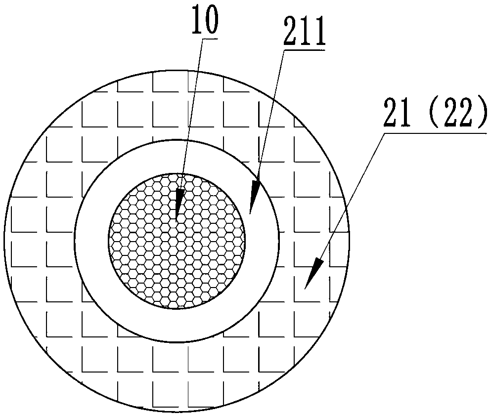
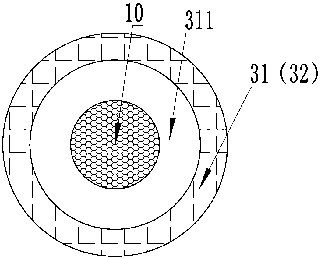
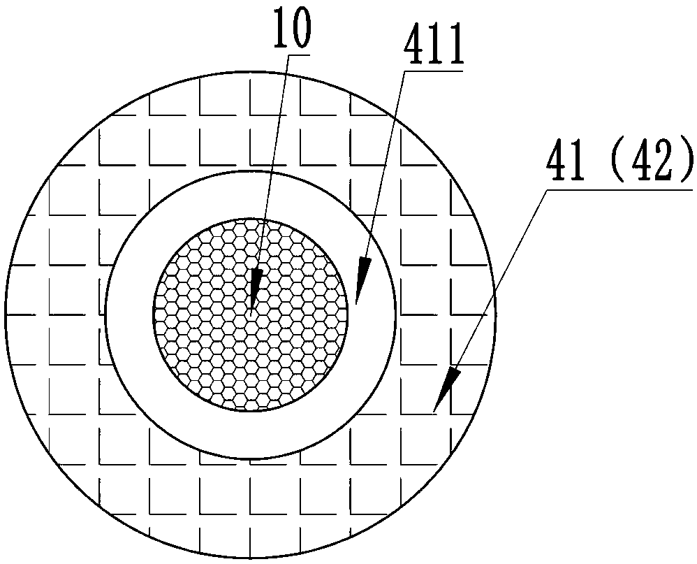
The invention discloses a secondary soldering resistance method and a thick copper plate structure of a thick copper plate. The method comprises the following steps: providing a thick copper plate with a soldering resistance layer to be printed; A first resist welding is carried out on the thick copper plate, and a first film is used for alignment exposure in the first resist welding process; Thefirst film chip is provided with a first opening window, and the area of the first opening window is a first opening area S1; Performing a second resistance welding on the thick copper plate which completes the first resistance welding, and performing alignment exposure by using a second film sheet in the second resistance welding process; The second film chip is provided with a second opening window, and the area of the second opening window is a second opening area S2; The first window area S1 is larger than the second window area S2. The invention enlarges the window area of the first filmused in the first soldering resistance process of the thick copper plate, and reduces the phenomenon of soldering resistance upper pad when the thick copper plate is soldered.

Description

technical field [0001] The invention relates to the field of circuit boards, in particular to a secondary solder resist method for a thick copper plate and a thick copper plate structure. Background technique [0002] In the circuit board layout design, the copper thickness of the inner and outer layers is usually 1 / 3OZ or 0.5OZ. With the rapid development of electronic technology, the demand for thick copper (the thickness of the inner and outer layers of copper is greater than 3OZ) printed boards has undergone tremendous changes. , the application of thick copper foil boards is not limited to power substrates, but also extends to automotive electronic products, LED substrates, module substrates, etc. It plays an irreplaceable important role in the manufacture of substrates with high current and high heat dissipation requirements. [0003] The solder mask production of thick copper boards is one of the bottleneck processes in the processing of thick copper PCBs. Due to the...

Claims


Application Information

Patent Timeline
IPC IPC(8): H05K3/28
CPCH05K3/282H05K2203/052
Inventor 吴华军蔡志浩邵勇朱占植梁高
Owner SHENZHEN WUZHU TECH
Learn More