A weakly physically non-clonable function circuit utilizing PMOS process deviations

A technology of process deviation and functional circuit, which is applied in the field of weak physical non-clonable functional circuit, can solve the problems that MOS tube cannot adopt the minimum process size, the area of ​​weak PUF circuit is large, and the key cannot be reset, so as to achieve compact layout area and low power consumption. Low, simple structure effect

Active Publication Date: 2019-01-18
NINGBO UNIV
View PDF7 Cites 8 Cited by
  • Summary
  • Abstract
  • Description
  • Claims
  • Application Information

AI Technical Summary

Problems solved by technology

However, the weak PUF circuit implemented by the SRAM-PUF unit disclosed in Document 1 has the following problems: 1. The key generated after the SRAM-PUF is powered on cannot be reset; 2. The SRAM-PUF unit contains 6 MOS transistors (2 PMOS tube and 4 NMOS tubes), the number of MOS tubes used is large, and in order to ensure that the SRAM-PUF unit can be read and written normally, the 6 MOS tubes need to use ratio logic, so that the MOS tubes cannot use the minimum process size, and the 6 There are both PMOS transistors and NMOS transistors in the MOS transistors, which ultimately leads to a large area of ​​the weak PUF circuit implemented by the SRAM-PUF unit and high power consumption.
Although the weak PUF circuit realized by the SRAM-PUF unit with reset function disclosed in Document 2 has a reset function, it also has the following problems: 1. The SRAM-PUF unit with reset function includes 10 MOS transistors ( 4 PMOS tubes and 6 NMOS tubes), the number of MOS tubes used is large, and there are both PMOS tubes and NMOS tubes in the 10 MOS tubes, which eventually leads to the weak PUF realized by the SRAM-PUF unit with reset function The circuit area is large and the power consumption is high; Second, due to the stacking effect of the PMOS tube, the node 'Q / QB' takes a long time to transition from the transient state to the bistable state, which has a negative impact on the speed

Method used


Image

  • A weakly physically non-clonable function circuit utilizing PMOS process deviations
  • A weakly physically non-clonable function circuit utilizing PMOS process deviations
  • A weakly physically non-clonable function circuit utilizing PMOS process deviations

Examples


Embodiment 1

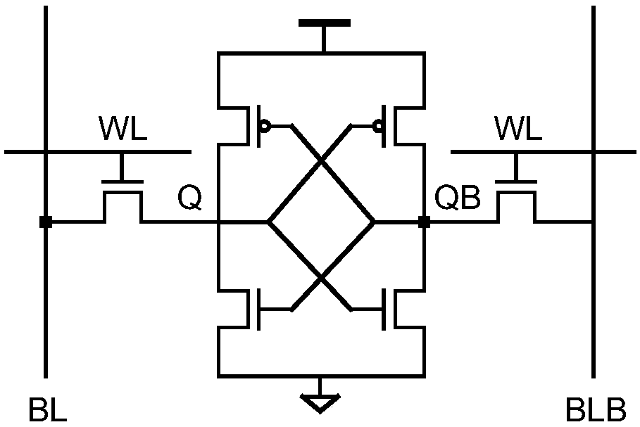
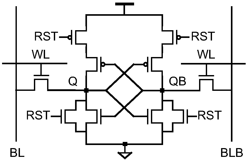
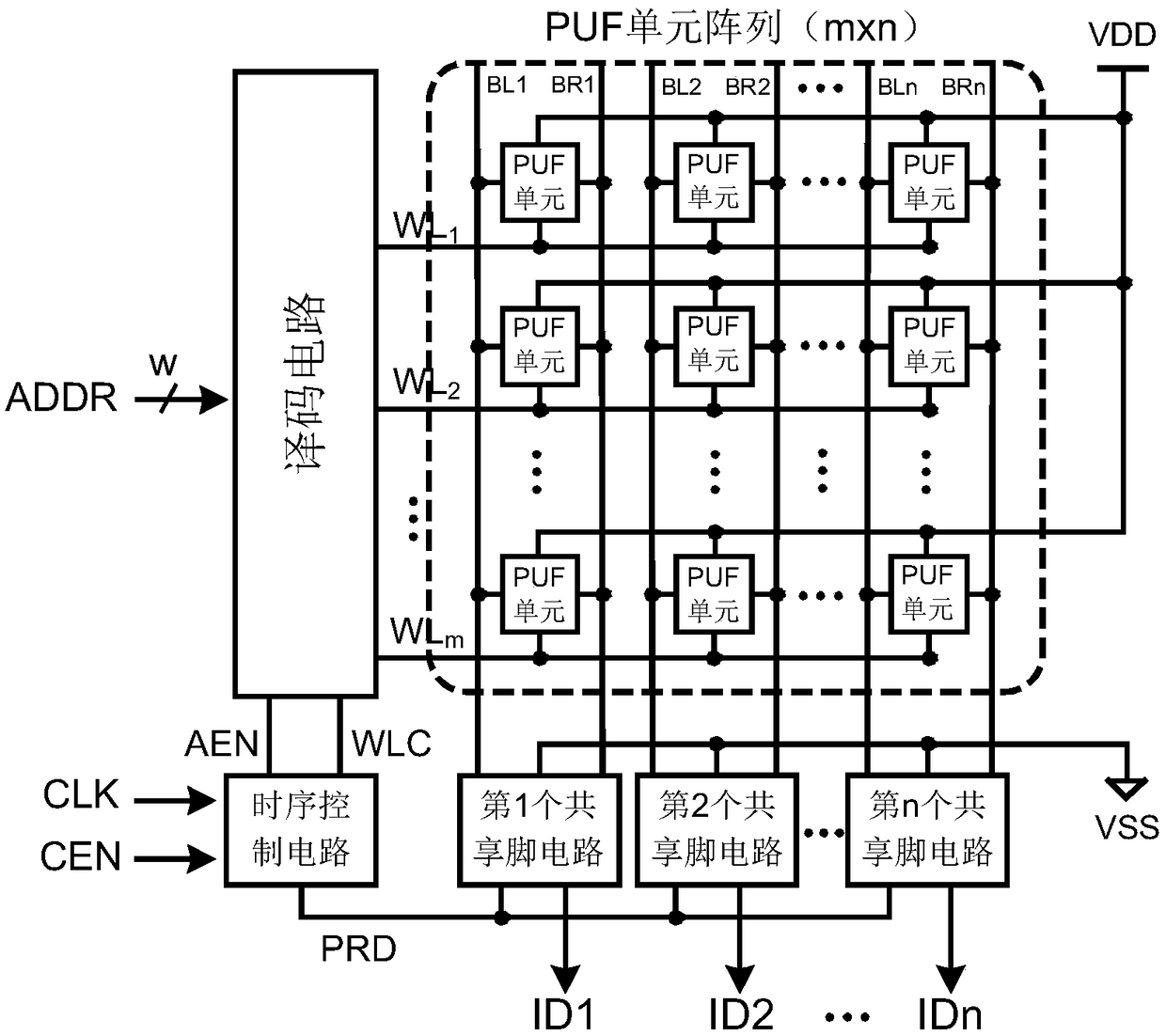
[0023] Example one: such as figure 2 , image 3 with Figure 4 As shown, a weak physical unclonable function circuit using PMOS process deviation includes a decoding circuit, a timing control circuit, a PUF unit array and n shared pin circuits with the same structure. The PUF unit array consists of m×n The PUF unit is arranged in m rows and n columns, and × is the symbol of multiplication operation. The decoding circuit has w-bit input, m-bit output, controlled clock signal input and word line control signal input, and timing control circuit It has an enable signal input terminal, a clock signal input terminal, a pre-discharge signal output terminal, a controlled clock signal output terminal, and a word line control signal output terminal. Each shared pin circuit has a pre-discharge signal input terminal, an output terminal, and a first Bit line connection end, second bit line connection end, each PUF unit has a word line connection end, a first bit line connection end and a sec...

Embodiment 2

[0026] The second embodiment: this embodiment is basically the same as the first embodiment, the difference lies in:

[0027] In this embodiment, such as Figure 5 As shown, the timing control circuit includes a latch LH1, a first two-input AND gate A1, a delay chain, a second two-input AND gate A2, and a buffer BF1; the latch LH1 has a clock terminal, an input terminal and an output terminal, The first two-input AND gate A1 and the second two-input AND gate A2 have a first input terminal, a second input terminal and an output terminal respectively. The input terminal of the latch LH1 is the enable signal input terminal of the timing control circuit. The clock terminal of the LH1 is connected to the second input terminal of the first two-input AND gate A1 and its connection terminal is the clock signal input terminal of the timing control circuit, the output terminal of the latch LH1 and the first two-input AND gate A1 One input is connected, the first two input and the output of...


PUM


Abstract

The invention discloses a weak physical non-clone function circuit utilizing PMOS process deviation, including a decoding circuit, a sequencing circuit, an array of PUF cells and n shared pin circuits, The PUF cell array is formed by arranging m * n PUF cells in m rows and n columns, the PUF unit includes a first PMOS transistor, second PMOS transistor, third PMOS transistor and fourth PMOS transistor and the width-to-length ratios of the four PMOS transistors are all minimum sizes in the TSMC 65 nm process: 120 nm / 60 nm, each share pin circuit comprises a first NMOS transistor, a second NMOStransistor, a third NMOS transistor, a fourth NMOS transistor, a first two-input NAND gate and a second two-input NAND gate, and that width-to-length ratio of the four NMOS transistor ranges from 2 mum / 60 nm to 8 mum / 60 nm; The circuit has the advantages of small area, low power consumption, small delay and high speed on the basis of the reset function.

Description

Technical field [0001] The invention relates to a physical unclonable function circuit, in particular to a weak physical unclonable function circuit using PMOS process deviation. Background technique [0002] Physical Unclonable Function (PUF) can guarantee information security at the chip physical level, so it has received more and more attention. The physical unclonable function circuit is a very promising embedded key generation circuit, which can generate a series of output keys with randomness, uniqueness and unclonability by capturing the random process deviation of the PUF unit. These output keys can be used in the field of information security, such as key generation, device authentication, and IP protection. [0003] At present, physical unclonable function circuits are usually divided into two categories: weak PUF circuits and strong PUF circuits. In a weak PUF circuit, each PUF unit usually produces a one-bit output response, and the output responses of each PUF unit c...

Claims


Application Information

Patent Timeline
Patent Type & Authority Applications(China)
IPC IPC(8): G06F21/73
CPCG06F21/73H03K19/00315G06F1/10G06F21/75
Inventor 汪鹏君李刚张会红张跃军
Owner NINGBO UNIV
Why Eureka
Try Eureka