OLED display substrate and manufacturing method thereof, and OLED display device
A display substrate and substrate substrate technology, which is applied in semiconductor/solid-state device manufacturing, semiconductor devices, electrical components, etc., can solve the problems of large volume occupied by OLED displays and the inability to meet the thinning and thinning of OLED displays.
- Summary
- Abstract
- Description
- Claims
- Application Information
AI Technical Summary
Problems solved by technology
Method used
Image

Examples
Embodiment 1
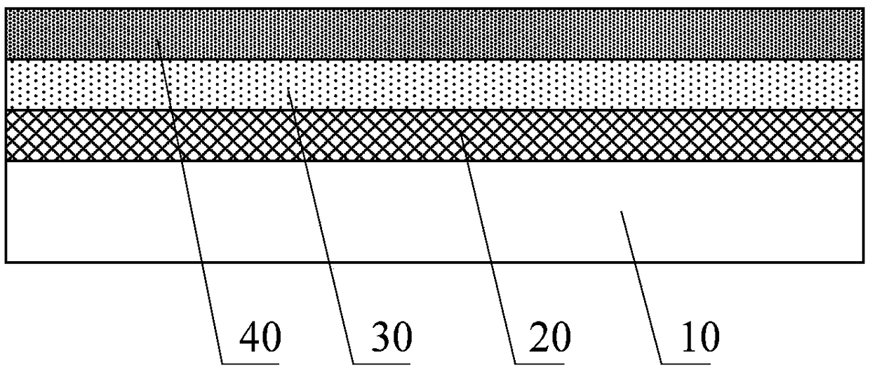
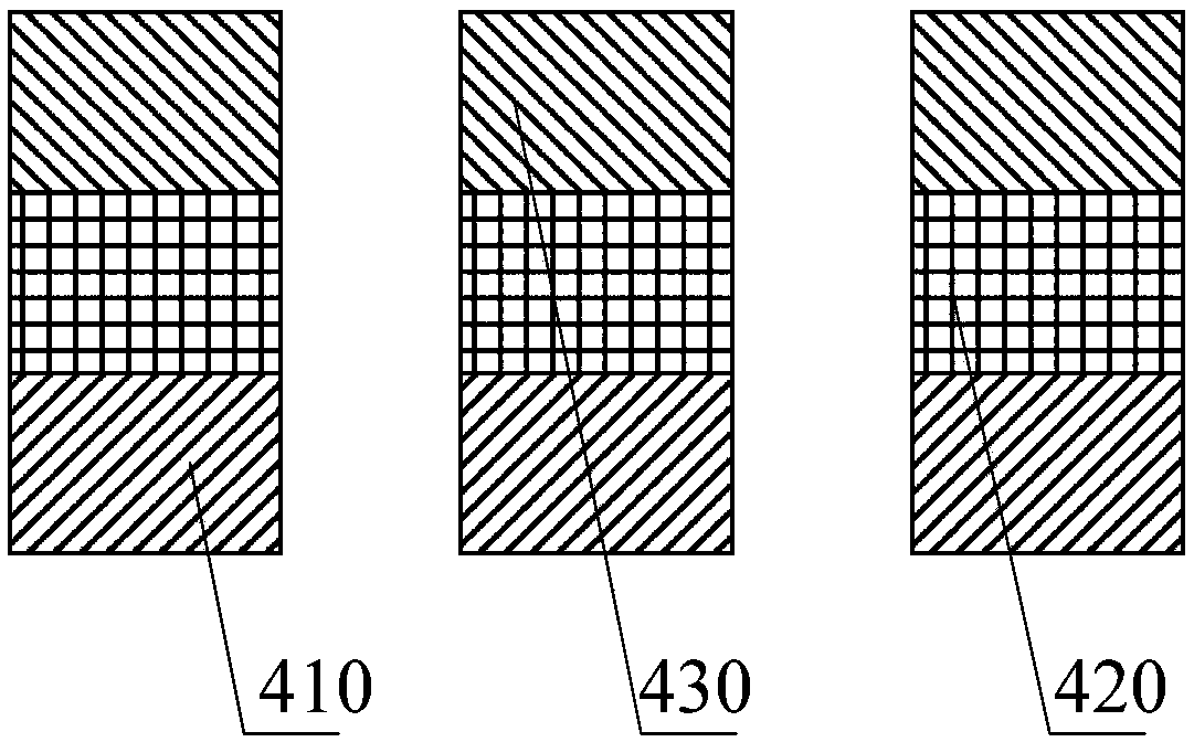
[0072] figure 1 Schematic diagram of the structure of an OLED display substrate provided by an embodiment of the present invention Figure one ,Such as figure 1 As shown, the embodiment of the present invention provides an OLED display substrate, including: a base substrate 10, an OLED device layer 20 disposed on the base substrate 10, and an encapsulation layer 30 for encapsulating the OLED device layer 20. The OLED display substrate also Includes: piezoelectric functional layer 40.
[0073] Specifically, the piezoelectric functional layer 40 is disposed on the side of the packaging layer 30 away from the base substrate 10, and is used to generate mechanical vibration under the action of electrical signals to generate ultrasonic waves or audible sound waves.
[0074] Optionally, the base substrate 10 is made of materials including glass, plastic, quartz, polyimide, etc., which are not limited in the embodiment of the present invention.
[0075] Specifically, the OLED device layer 20...
Embodiment 2
[0122] Based on the inventive concept of the foregoing embodiment, the embodiment of the present invention also provides a method for manufacturing an OLED display substrate. Figure 14 It is a flowchart of a manufacturing method of an OLED display substrate provided by an embodiment of the present invention, such as Figure 14 As shown, the manufacturing method of the OLED display substrate provided by the embodiment of the present invention specifically includes the following steps:
[0123] Step 100: Provide a base substrate.
[0124] Optionally, the manufacturing material of the base substrate includes: glass, plastic, quartz, polyimide, etc., which is not limited in the embodiment of the present invention.
[0125] Step 200, forming an OLED device layer on a base substrate.
[0126] Specifically, the OLED device layer includes a thin film transistor and an anode, a light emitting layer, and a cathode disposed on the thin film transistor. The thin film transistor includes an active...
Embodiment 3
[0172] Based on the inventive concept of the foregoing embodiment, an embodiment of the present invention also provides an OLED display device, including an OLED display substrate.
[0173] Among them, the OLED display substrate is the OLED display substrate provided in the first embodiment, and its implementation principles and effects are similar, and will not be repeated here.
[0174] Specifically, the OLED display device may be any product or component with a display function, such as an OLED panel, a mobile phone, a tablet computer, a television, a monitor, a notebook computer, a digital photo frame, a navigator, and the like.
[0175] The drawings of the embodiments of the present invention only relate to the structures involved in the embodiments of the present invention, and other structures can refer to the usual designs.
[0176] For clarity, in the drawings used to describe the embodiments of the present invention, the thickness and size of layers or microstructures are exa...
PUM
 Abstract
Description
Claims
Application Information
 - R&D
- Intellectual Property
- Life Sciences
- Materials
- Tech Scout
- Unparalleled Data Quality
- Higher Quality Content
- 60% Fewer Hallucinations
Browse by: Latest US Patents, China's latest patents, Technical Efficacy Thesaurus, Application Domain, Technology Topic, Popular Technical Reports.
© 2025 PatSnap. All rights reserved.Legal|Privacy policy|Modern Slavery Act Transparency Statement|Sitemap|About US| Contact US: help@patsnap.com